Electro-Thermal Simulation Tutorial: Self-Heating in OghmaNano (Part A)
1. Introduction
Self-heating is a defining feature of operating electronic and optoelectronic devices. Whenever current flows, electrical power is dissipated and converted into heat, raising the local device temperature. That temperature rise feeds directly back into transport, recombination, and trapping through the strong temperature dependence of material parameters. Electro-thermal simulation is the self-consistent treatment of this coupled electrical–thermal problem.
In practice, self-heating arises from multiple physical mechanisms acting simultaneously. Carrier transport heating converts electrical energy into heat as charge carriers move through spatially varying band-edge energies, encompassing both Joule heating in homogeneous regions and Peltier heating or cooling at interfaces. Carrier recombination transfers electronic energy directly to the lattice, while additional heat is generated by parasitic series and shunt losses. Accurately capturing device behaviour under bias therefore requires all heat-generation terms to be evaluated self-consistently from the electrical solution and fed back through a thermal diffusion model.
An electro-thermal simulation therefore consists of two coupled solves, reflecting the fact that the electrical and thermal problems typically operate on very different physical length scales:
- a fully coupled electrical transport solve (drift–diffusion, Poisson, recombination, and traps), usually confined to the electrically active region of the device, and
- a thermal diffusion solve for the lattice temperature field, which may extend well beyond the active region into contacts, substrates, and heat sinks.
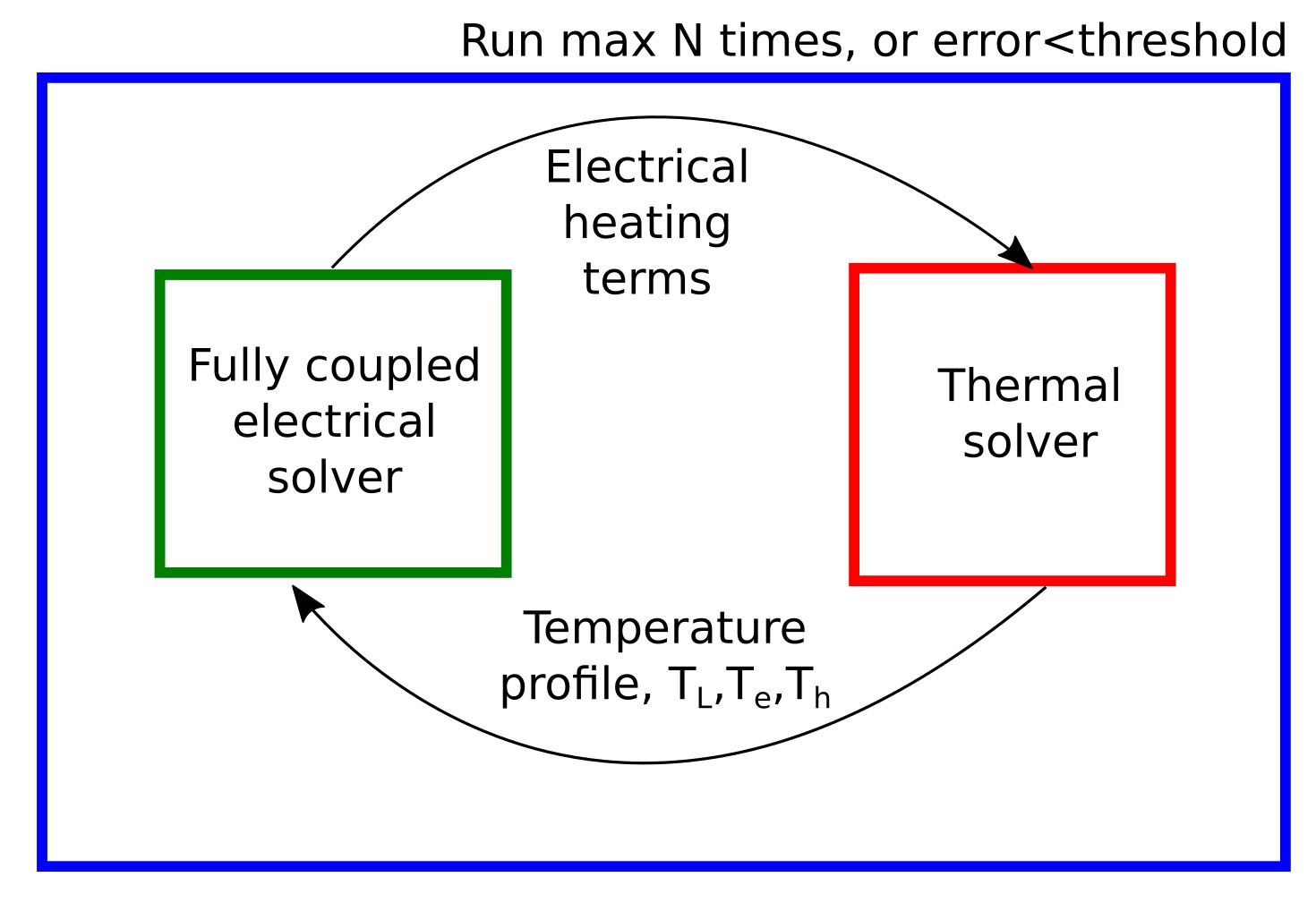
The coupling strategy implemented in OghmaNano is illustrated in ??. At a given applied voltage, the electrical equations are solved using the current temperature field. Heat-generation terms are then evaluated and passed to the thermal solver, which updates the lattice temperature. This outer iteration continues until the electrical and thermal residuals both satisfy the convergence criteria.
In this tutorial, you will run a fully coupled electro-thermal simulation, identify the active heating mechanisms, and examine how the lattice temperature evolves with applied voltage. This establishes the electro-thermal workflow that will be extended in Part B to detailed thermal meshes, boundary conditions, and spatial heat-distribution analysis.
2. Open the thermal example
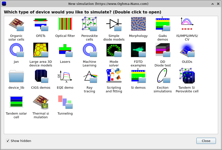
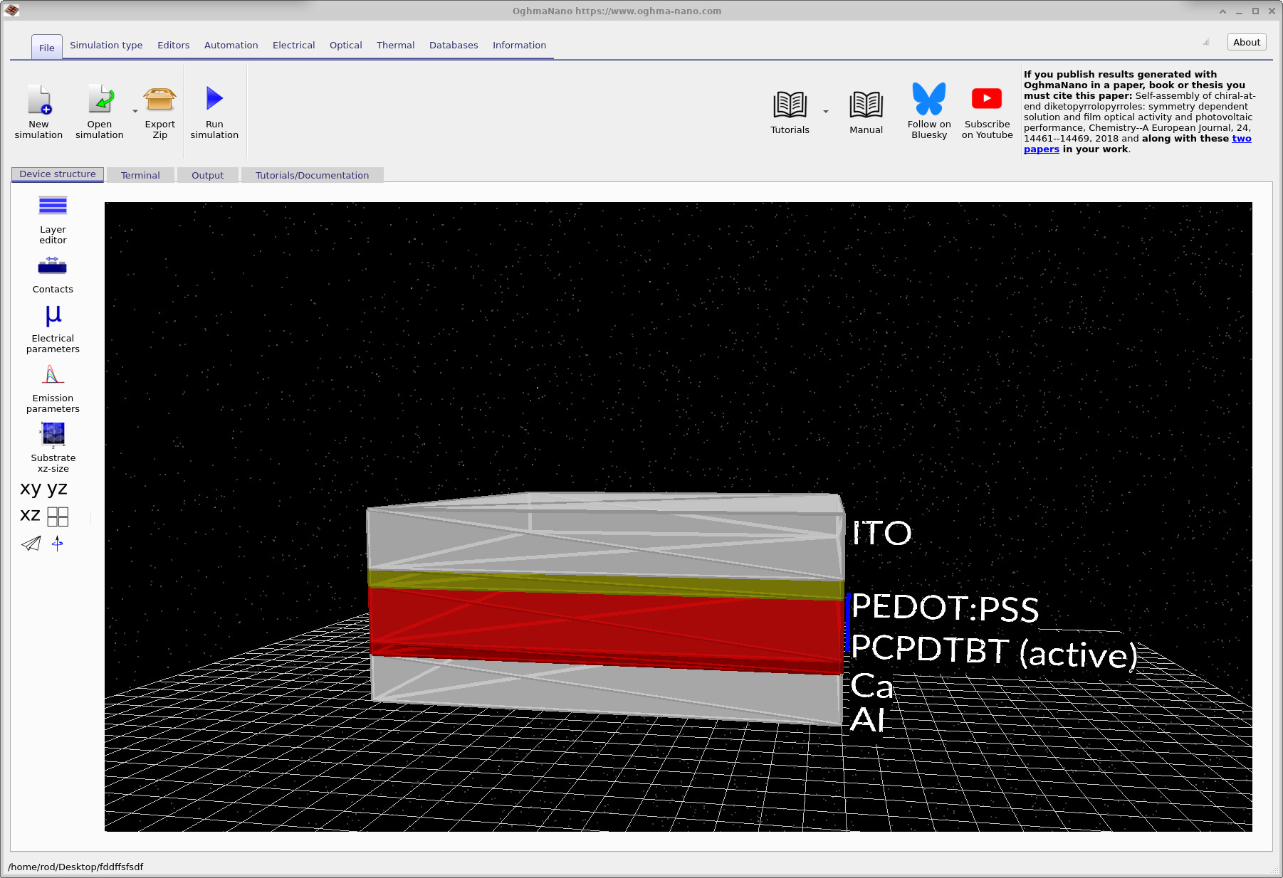
From the main OghmaNano window, click New simulation. In the device library, double-click Thermal simulation (the small candle icon in the bottom-left), shown in ??. This loads a complete electro-thermal example project with the thermal model and solver coupling already configured. After opening the example, the main simulation interface is displayed (??). The device is a multilayer diode stack with injection, transport, and recombination, chosen because it produces realistic current densities and measurable self-heating under bias. While the materials here correspond to an organic architecture, the purpose of the example is to demonstrate the electro-thermal workflow itself, not material-specific physics.
Before running the simulation, click Electrical parameters in the main window to open the electrical parameter editor (??). This view lists the transport, recombination, and trap parameters used by the electrical solver, which together define the current density and recombination profiles that generate heat during the electro-thermal simulation. At this stage, no parameters need to be modified.
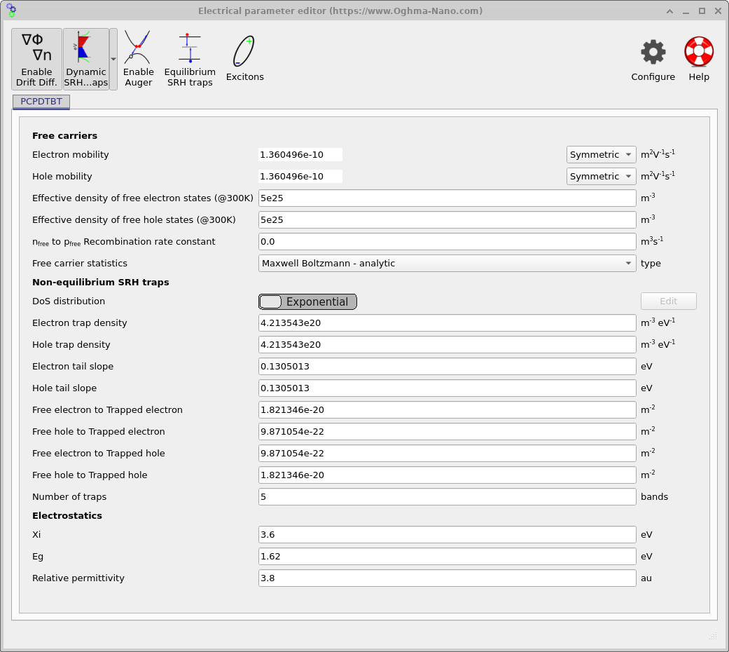
In this example, the electrical parameters were obtained by fitting the coupled electro-thermal model to experimental measurements reported in In Situ Visualization and Quantification of Electrical Self-Heating in Conjugated Polymer Diodes Using Raman Spectroscopy (S. Maity, C. Ramanan, F. Ariese, R. C. I. MacKenzie, E. von Hauff, Adv. Electron. Mater., 2021, 2101208; https://doi.org/10.1002/aelm.202101208 ). As a result, several parameters appear with multiple decimal places; this reflects the numerical endpoint of the fitting procedure rather than an implication of absolute parameter accuracy. Such fitting is not required for general electro-thermal modelling: for most devices, standard literature parameters or reasonable nominal values are sufficient to obtain physically meaningful insight into heating mechanisms, temperature rise, and electro-thermal coupling, with parameter fitting only necessary when quantitative agreement with a specific experiment is required.
3. Examining the thermal ribbon (enabled heat sources)
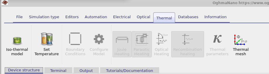
Before running the simulation, navigate to the Thermal ribbon in the main window. The candle icon provides a simple state indicator: a lit candle indicates that the thermal model is enabled, while an unlit candle indicates that the simulation will run at fixed temperature. The two states are shown in ?? and ??. When the thermal model is enabled, multiple heat-generation mechanisms can be activated. Each enabled term contributes to the total volumetric heat source used by the thermal solver. In this example, the following mechanisms are included:
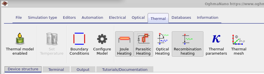
- Drift heating (labelled Joule heating in the ribbon), including thermo-electric effects
- Parasitic heating, arising from series and shunt resistive losses
- Recombination heating, due to energy transfer from carriers to the lattice
- Optical heating, available when optical absorption is converted into heat
The ribbon also provides access to Thermal parameters, Thermal mesh, and Boundary conditions. These controls are important because the thermal problem is typically defined on a much larger physical domain than the electrical problem. Their role is discussed in detail in Section 6 and in Part B.
3.1 Drift heating (Joule and Peltier contributions)
The drift-related heat source used in OghmaNano is written as:
\[ Q_{\mathrm{drift}} = \mathbf{J}_n \cdot \nabla E_C + \mathbf{J}_p \cdot \nabla E_V \]
This form captures both conventional resistive Joule heating and thermo-electric (Peltier-like) effects associated with spatial variations in carrier energy. In regions dominated by resistive transport, the term is positive and corresponds to heat generation. Near interfaces or in regions of strong band bending, local negative contributions may occur, corresponding to carrier-induced cooling or heating of the lattice. The presence of both positive and negative regions in drift-heating plots is therefore expected and reflects the local energy balance rather than numerical noise.
3.2 Parasitic heating (series and shunt losses)
In addition to intrinsic transport and recombination processes, practical devices dissipate energy in series and shunt resistive elements. In the electro-thermal model, these losses are represented directly as a volumetric heat-generation term:
\[ Q_{\mathrm{parasitic}} = \frac{I^2 R_s + \dfrac{V^2}{R_{sh}}}{V_{\mathrm{dev}}} \]
Here, \(V_{\mathrm{dev}}\) is the volume over which the parasitic dissipation is distributed. Because the microscopic location of parasitic losses is generally not resolved by the electrical model, this contribution is treated as a spatially distributed heat source, ensuring global energy conservation without introducing assumptions about unresolved hot-spot locations.
3.3 Recombination heating
Carrier recombination transfers electronic energy to the lattice. In this model, the corresponding heat-generation term is written as:
\[ Q_{\mathrm{rec}} = \left(\langle w_n \rangle + E_g + \langle w_p \rangle \right)\,R \]
Here, \(R\) is the recombination rate, while \(\langle w_n \rangle\) and \(\langle w_p \rangle\) represent average carrier energy contributions relative to the band edges. The bandgap \(E_g\) sets the dominant energy scale. Because recombination is often spatially localised, recombination heating typically exhibits a different spatial distribution from drift-related heating, making it useful to analyse these contributions separately.
Other thermal controls available in the ribbon are examined in detail in Part B. For Part A, the objective is simply to identify which heat sources are enabled and to understand their physical interpretation before running the simulation.
4. Run the electro-thermal simulation
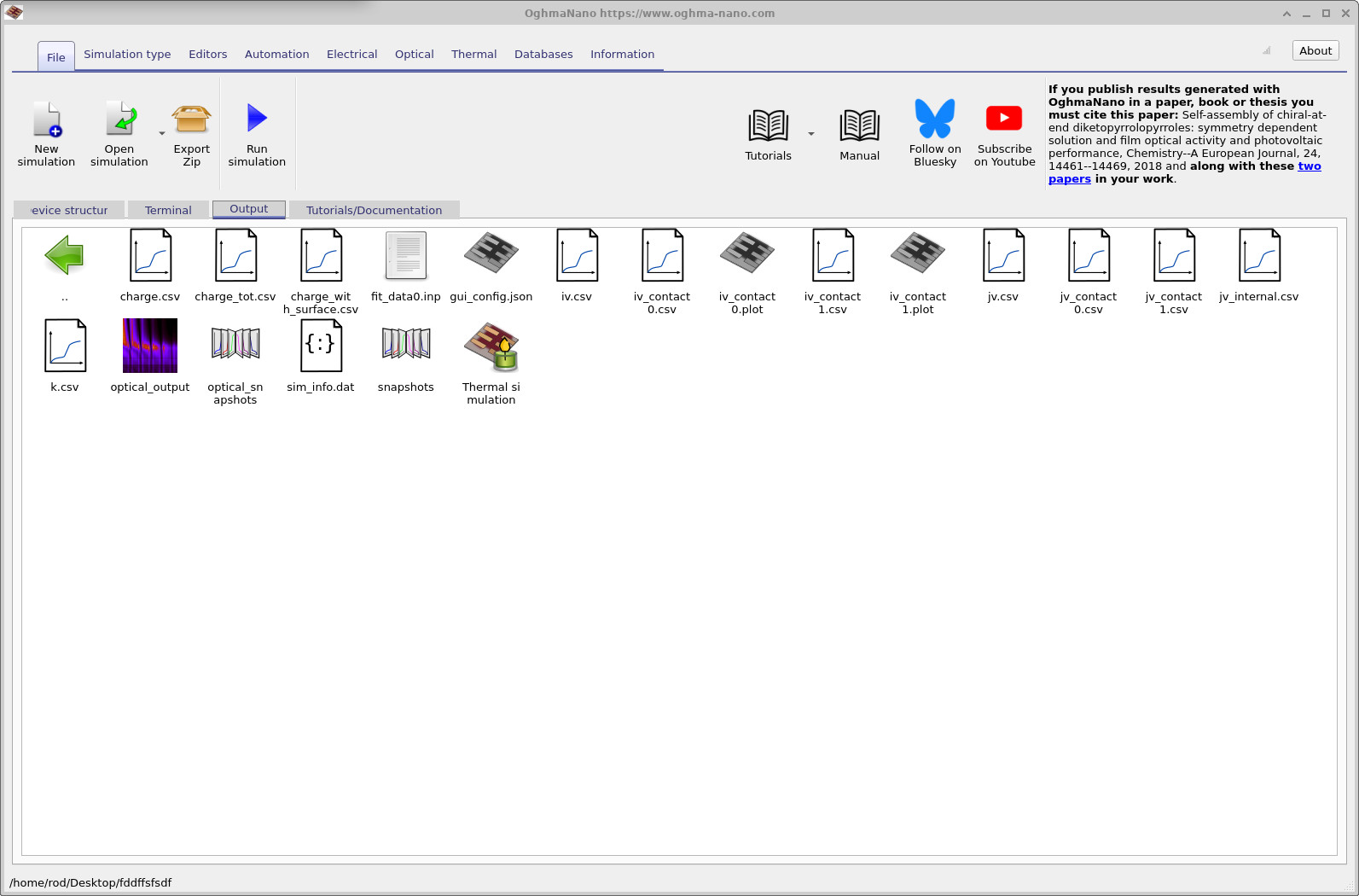
Run the simulation by pressing the blue Run simulation button in the main window (or press F9). After the run completes, all results are written to the output directory shown in ??.
The electro-thermal run produces the standard electrical outputs, such as the current–voltage (JV) curve, together with additional thermal outputs. In particular, alongside the JV characteristic (??), a voltage-dependent lattice temperature output is generated (??), representing the self-consistent temperature of the device under bias.
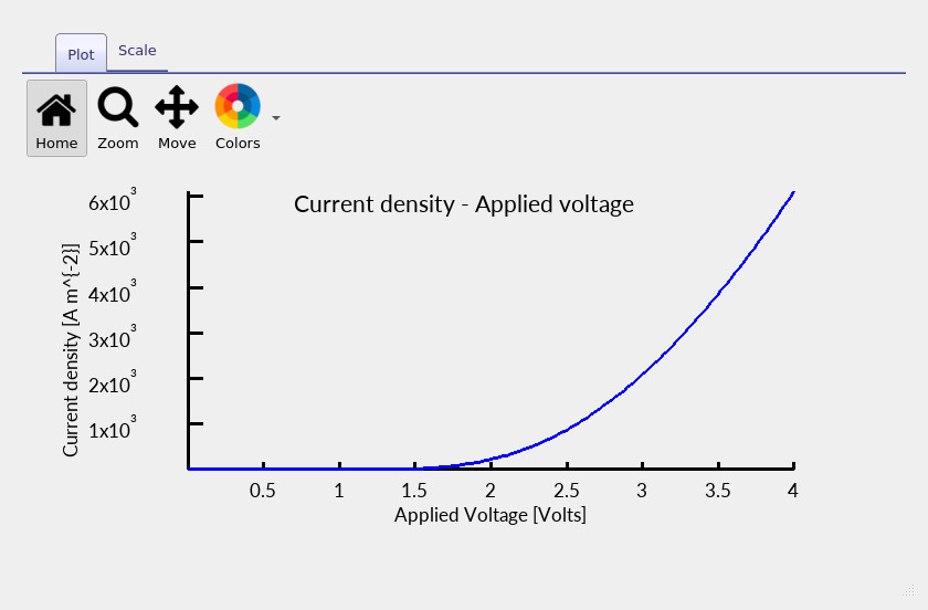
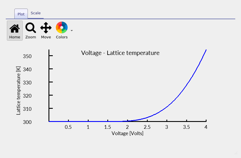
In an electro-thermal simulation, the JV curve is no longer evaluated at a fixed lattice temperature. Instead, the temperature is determined self-consistently at each bias point through the coupled electrical–thermal solve. Once a device turns on, the dissipated power \(P \sim IV\) can increase rapidly, and the resulting temperature rise can measurably modify transport and recombination parameters, leading to observable changes in JV slope and curvature.
5. Examining microscopic heating and heat sources
We now examine the microscopic heat generation terms inside the device.
These quantities resolve where electrical energy is converted into heat and
which physical mechanism is responsible. To access these plots, double-click the
snapshots folder in the Output tab (as used previously for
electrical snapshots). This opens the Snapshots viewer, shown in
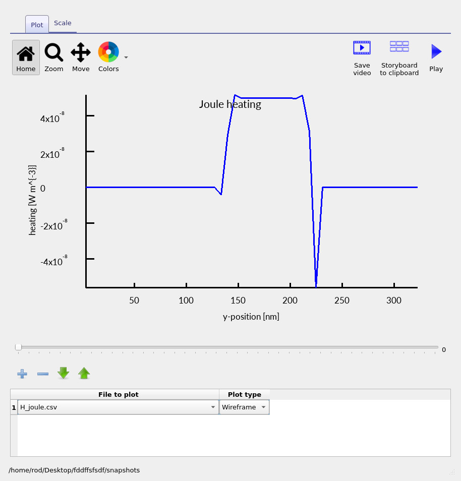
??. Click the + button and select H_joule.csv. This displays the spatial distribution of the carrier transport heating term. By moving the
slider bar at the bottom of the window, the evolution of this heating profile with applied
voltage can be explored.
The transport heating term shown here corresponds to the current-induced heat source defined earlier (see the governing equation above). It represents the conversion of electrical energy into heat as charge carriers move through spatially varying band-edge energies. Because the current density includes both drift and diffusion components, this term naturally captures the full transport contribution rather than a purely field-driven process. In regions where band edges vary smoothly and transport is resistive, the contribution is positive and corresponds to conventional Joule heating. At interfaces or in regions with strong band-edge gradients, the same term may become negative, corresponding to Peltier heating or cooling associated with carrier energy exchange at heterojunctions.
?? shows the transport heating at lower bias, where both heating and cooling regions are present. At higher bias, shown in ??, the current density increases and the transport heating becomes uniformly positive, making Joule heating a dominant contribution to the overall energetic losses in the device.

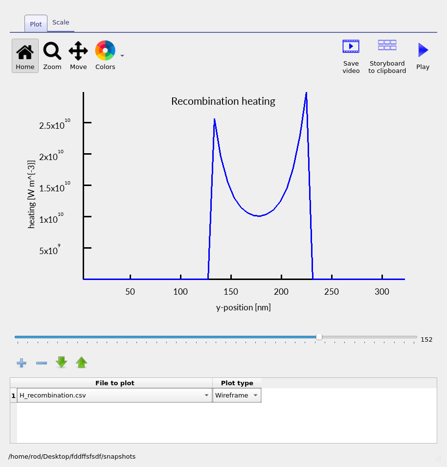

Recombination heating is shown in ??. This term follows the spatial distribution of carrier recombination and highlights regions where electron–hole annihilation transfers energy directly to the lattice. Finally, ?? shows the parasitic heating contribution. This term represents power dissipated in series and shunt resistances. Because the microscopic location of this dissipation is generally unknown, it is distributed uniformly across the electrically active region of the device by construction.
Together, these plots demonstrate that different physical mechanisms dominate heat generation in different regions of the device and at different operating biases. Electro-thermal simulation allows these contributions to be separated, visualised, and analysed individually.