Electro-Thermal Simulation Tutorial (Part B): Thermal Mesh, Boundary Conditions, and Experimental Fits
1. Introduction: scope and focus of Part B
In Part A you ran an electro-thermal simulation, identified the principal heat-generation mechanisms (carrier transport heating, recombination heating, and parasitic losses), and learned how to extract lattice temperature outputs as a function of applied bias. That first part focused on what heat is generated and where it appears in the device. In this Part B, we focus on the other half of the problem: how heat is transported away from the device. This is governed by the thermal mesh and, critically, by the thermal boundary conditions. Boundary conditions encode how the device is mounted, cooled, or heat-sunk in practice, and they often have a first-order impact on the resulting temperature rise. Two simulations with identical electrical behaviour and identical heat-generation terms can produce very different temperature profiles purely because of different thermal boundary assumptions.
You will therefore see why electro-thermal simulation typically uses a thermal domain that is larger than the electrical domain, how effective boundary conditions are used to represent macroscopic heat sinks without explicitly meshing them, and why temperature-dependent material quantities are precomputed on a discrete temperature grid. This tutorial continues to use an organic diode example because it is experimentally grounded and includes measurable self-heating effects, but the workflow is completely general. The same concepts apply to inorganic semiconductors, thin-film devices, power electronics, photodetectors, and any structure where electrical power dissipation feeds back into transport through temperature.
By the end of Part B, you should understand:
- why the thermal mesh is distinct from the electrical mesh,
- how thermal boundary conditions control heat extraction,
- how temperature discretisation is used internally for efficiency, and
- why self-heating must sometimes be included to match experimental data.
2. Thermal mesh and boundary conditions
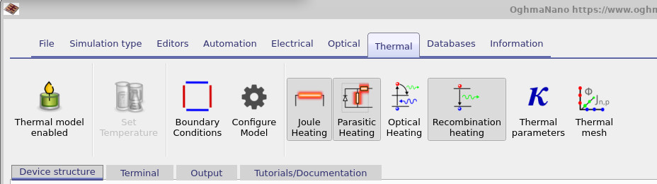
Start in the main simulation window and navigate to the Thermal ribbon. This is the same ribbon introduced in Part A: it contains the heating-source toggles and the core configuration controls (thermal parameters, thermal mesh, and boundary conditions). The ribbon is shown in ??.
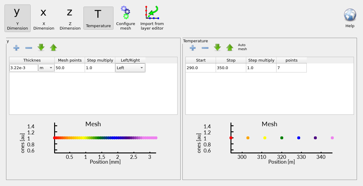
2.1 The thermal mesh and why it is not the electrical mesh
Click Thermal mesh to open the thermal mesh editor. At first glance it looks like the mesh editors you have seen elsewhere in OghmaNano, but it is solving a different physical problem: heat diffusion. The key point is that electro-thermal simulation uses two meshes, because the electrical and thermal problems usually live on fundamentally different length scales:
- The electrical mesh solves transport (drift–diffusion + Poisson + recombination/traps). It is typically focused where the electrical action is strongest: the active layer and nearby interfaces, where fields and carrier densities vary rapidly. Those variations can occur on nanometre to micron scales.
- The thermal mesh solves the lattice heat equation. Heat does not stop at the active layer: it spreads through the entire stack, into contacts, substrates, packaging, and toward whatever removes heat from the device. Those pathways are commonly on millimetre to centimetre scales.
This mismatch is why a single “shared mesh” is usually the wrong abstraction. The electrical problem needs high resolution in the active region; the thermal problem needs a domain large enough to represent the heat-flow pathway. For example:
- A thin-film diode might have an active layer thickness of 100–300 nm, but the substrate might be 0.5–1 mm thick (glass) and the mounting block or stage can be centimetres.
- A metal contact might be only tens of nanometres thick electrically, yet it can be the dominant lateral heat spreader thermally because its thermal conductivity is large compared to organic or oxide layers.
In this example, you can see that the Y height of the thermal domain spans the full device stack thickness rather than being constrained to the electrically active region. That is typical: thermal transport involves every layer that conducts heat, not just the layers where current flows. Next, we configure how heat is allowed to leave this thermal domain using boundary conditions. The mesh defines the region in which heat can diffuse; the boundary conditions define what happens at the edges of that region.
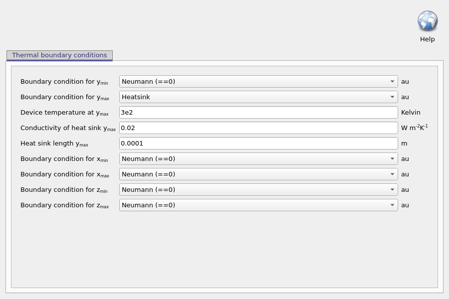
2.2 Boundary conditions: insulating faces and an effective heatsink
Open the boundary-condition editor shown in ??. In this example, most faces are set to Neumann (often shown as “Neumann (==0)”). Physically, a Neumann boundary condition specifies the normal heat flux at the boundary. When it is set to zero, it enforces:
\[ -k \nabla T \cdot \hat{n} = 0 \]
i.e. no heat flows through that boundary. These faces are treated as thermally insulating. This does not mean the device is thermally isolated overall; it simply tells the thermal solver that those boundaries are not part of the intended heat-removal pathway. The exception here is the ymax face, which is set to Heatsink. This boundary specifies a device temperature at ymax (here around 300 K), along with an effective heat-sink conductivity and a heat-sink length (on the order of a millimetre in this example).
Conceptually, this is an effective heat-removal model. It allows heat to flow out of the simulated device stack into a not-explicitly-meshed sink, without forcing the thermal mesh to include a macroscopic object. This matters because real heat sinks are typically orders of magnitude larger than thin-film devices: explicitly meshing a millimetre-to-centimetre scale sink at sub-micron resolution would be computationally inefficient and physically unnecessary. It is worth emphasising that, in thermal problems, boundary conditions largely determine how hot the device becomes. A poor heat-extraction pathway can cause the temperature to rise very rapidly, while an efficient pathway can keep the temperature close to ambient even under significant power dissipation.
A useful analogy is to think of the device as a bath being filled with water. The heat-generation terms are the tap: they pour energy into the system. The thermal boundary conditions are the plughole:
- If the plug is fully open (excellent heat extraction), the water level remains low.
- If the plug is partially blocked (limited heat extraction), the water level rises.
- If the plug is closed (no heat extraction), the bath will eventually overflow.
In this analogy, the water level is the lattice temperature. The purpose of thermal boundary conditions is therefore not cosmetic or secondary: they encode the physical environment that ultimately controls whether the device runs cool, warm, or catastrophically hot.
2.3 Temperature “mesh points” (why temperature is discretised)
The thermal mesh editor also shows a temperature range and a number of temperature points. This is not the spatial thermal mesh: it is the temperature grid used for precomputations. Many parts of the electrical/thermal model require temperature-dependent quantities to be evaluated repeatedly during the coupled solve, and it is computationally expensive to recompute them from scratch at every intermediate temperature. For example, depending on the chosen statistics and density-of-states model, the solver may need temperature-dependent relations for carrier densities, quasi-thermodynamic functions, and related lookup quantities. Rather than evaluating those “live” every time the coupled loop updates \(T_L\), OghmaNano precomputes background tables at a finite number of temperature points and then interpolates between them during the run. In this example the tables are generated at 7 points between 290 K and 350 K.
This makes the temperature range a modelling choice: it should comfortably bracket the temperatures expected during self-heating. If the device heats beyond the upper temperature, you risk extrapolation artefacts (or clamping depending on settings), which is rarely what you want. As a practical rule: choose a range that covers the anticipated operating temperatures with margin.
3. Thermal parameters (thermal conductivity and relaxation times)
In electro-thermal simulation, boundary conditions define how heat can leave the device, but material parameters define how heat moves within the stack. In practice, one of the most important quantities controlling temperature rise and hotspot formation is the thermal conductivity \(k\) (sometimes written \(\kappa\)).
To view or edit these parameters, open the Thermal ribbon and click Thermal parameters (the button marked with \(k\) / \(\kappa\)). This opens the layer-by-layer thermal parameter editor shown in ??.
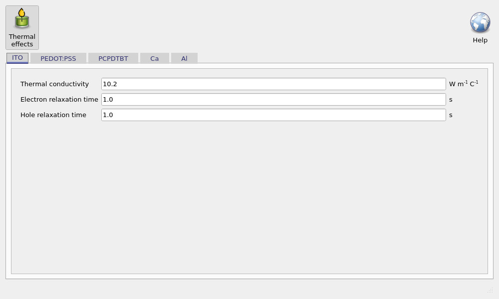
The editor exposes three key parameters for each layer:
- Thermal conductivity \(k\): governs how efficiently heat diffuses through that layer. Low-\(k\) layers act as thermal bottlenecks and can strongly increase the predicted lattice temperature rise.
- Electron relaxation time and hole relaxation time: these are only required when using the hydrodynamic / energy-transport model, where carrier temperatures can depart from the lattice temperature. In the standard lattice-heat model they are not needed because carrier temperatures are locked to \(T_L\).
In most workflows, the thermal conductivities are chosen from published values (or measured where available) and then refined only if there is a clear experimental justification. Together with boundary conditions, \(k\) is one of the main determinants of absolute device temperature and the spatial structure of hotspots.
4. How the coupled electro-thermal solver works (and why it is slower)
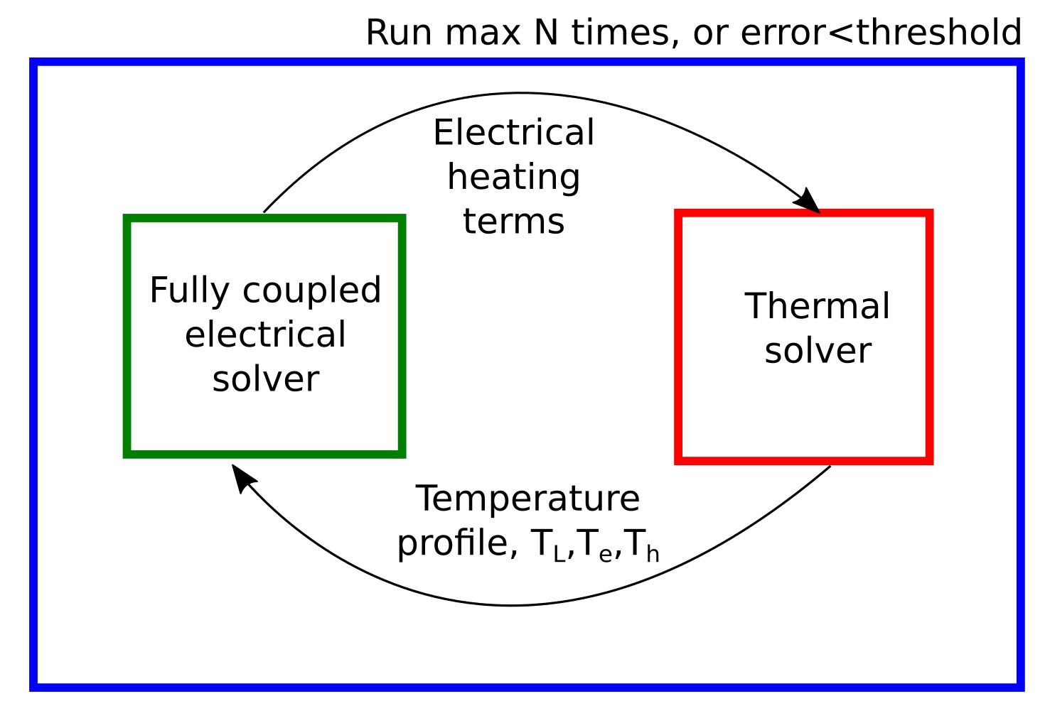
An electro-thermal simulation in OghmaNano consists of two coupled solvers:
- a fully coupled electrical solver (drift–diffusion and Poisson, including recombination and traps when enabled), and
- a thermal solver that solves the heat-diffusion equation for the lattice temperature field \(T_L\) using heat-generation terms computed from the electrical solution.
At a given applied voltage, the solver does not run these stages once in sequence. Instead, it executes a self-consistent outer loop:
- solve the electrical transport problem using the current temperature field,
- compute heat-generation terms (transport, recombination, parasitic, and optionally optical),
- solve the thermal diffusion problem to update \(T_L\), and
- repeat until both electrical and thermal residuals are converged.
This iterative coupling is why electro-thermal simulations are slower than purely electrical ones: for each bias point, the electrical Newton solve and the thermal solve may both run multiple times before the coupled system stabilises. The result is a genuinely self-consistent multi-physics solution, rather than an electrical calculation with temperature added as a post-processing step.
The coupling is essential because the electrical and thermal problems typically live on very different physical length scales. Electrical transport is dominated by the active region, where fields, carrier densities, and recombination rates vary rapidly. Thermal transport must account for the entire heat-flow pathway, including contacts, substrates, encapsulation, and heat sinks. This is why OghmaNano provides independent controls for the thermal mesh and thermal boundary conditions.
It is also important to recognise that the electro-thermal framework naturally involves multiple temperatures. In general, the model distinguishes between the lattice temperature \(T_l\), which describes the temperature of the atomic lattice, the electron temperature \(T_e\), and the hole temperature \(T_h\).
Electrons and holes are mobile carrier populations that can, in principle, have their own local energies, just as they have their own quasi-Fermi levels. In the standard electro-thermal model used here, the electron and hole temperatures are locked to the lattice temperature, so all subsystems share a single temperature field.
In extreme regimes, OghmaNano also supports a hydrodynamic transport model in which electron and hole temperatures are allowed to deviate from the lattice temperature. That advanced model is described elsewhere and is only required in specialised situations. For the majority of device simulations, including this tutorial, the lattice-based electro-thermal model is both appropriate and sufficient.
5. Self-heating and comparison with experiment
This example device has been compared to experimental data using the electro-thermal model. No fitting is performed in this tutorial. Instead, the existing comparison is used to illustrate how self-heating alters the electrical response of the device, and why a coupled electro-thermal treatment is required at higher operating currents.
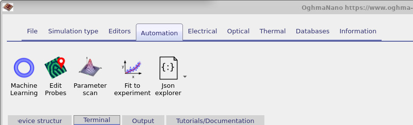
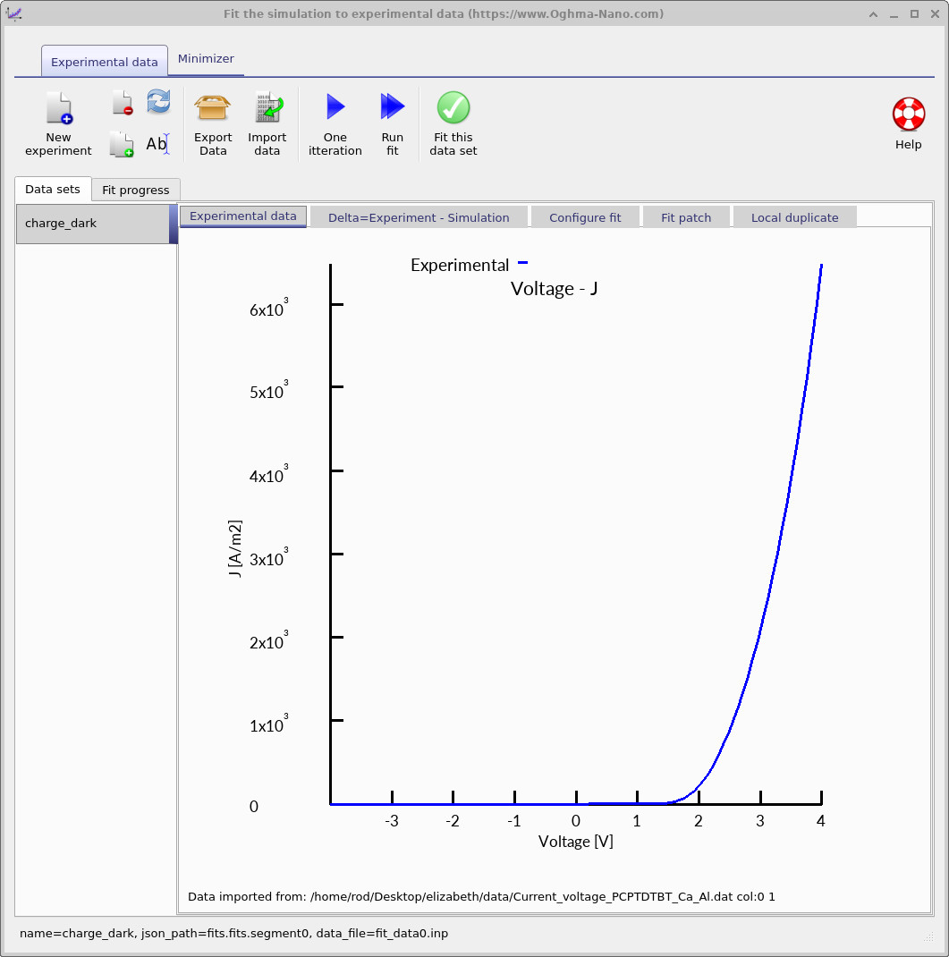
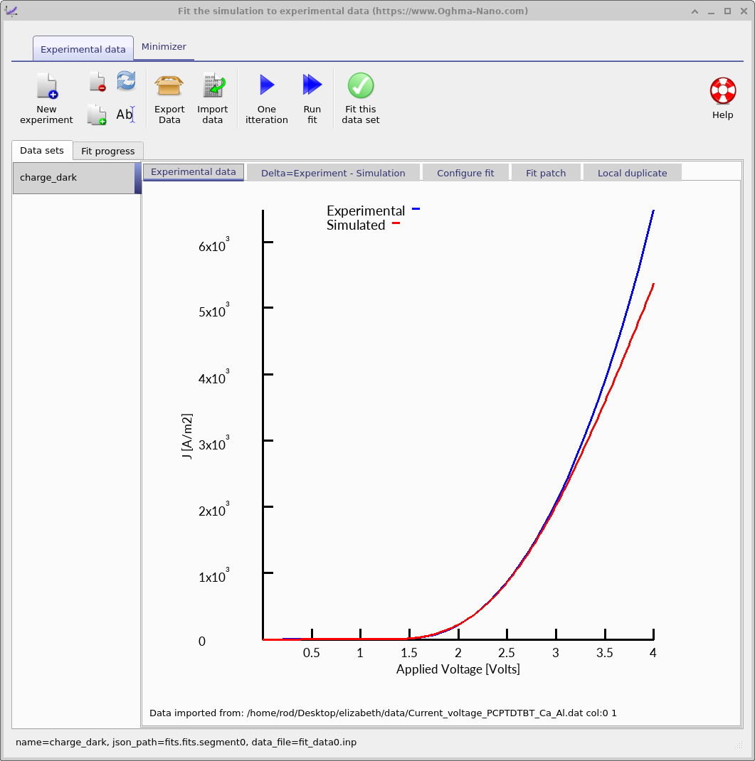
The comparison workflow is accessed via the Automation toolbar, shown in ??. Opening the fit-to-experiment tool displays the experimental JV data for this device, as shown in ??. This curve represents measured device behaviour under bias.
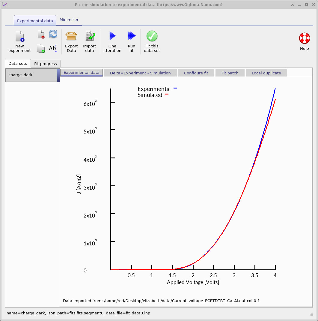
Run one iteration. After a single electro-thermal solve, the simulated JV curve is overlaid on the experimental data, as shown in ??. In this case, the agreement is close, indicating that the model captures the dominant transport and thermal physics of the device.
The role of self-heating becomes clear by repeating the same comparison with the thermal model disabled:
- Return to the Thermal ribbon.
- Disable the thermal model.
- Run one iteration of the comparison again.
The resulting JV curve no longer matches the experimental data, as shown in ??. The deviation is most pronounced at higher bias, where current densities are large and self-heating from carrier transport becomes significant.
This comparison demonstrates a central result of electro-thermal modelling: once devices operate in regimes of high current density, electrical power dissipation feeds back into transport through temperature rise. Fixed-temperature electrical simulations cannot capture this effect, whereas the coupled electro-thermal model can.