NMOS Capacitor Tutorial (Part B): Band Bending, Charge, and Surface Potential
1. Introduction
In Part A we focused on setting up and running a 2D NMOS capacitor simulation.
In this section we turn to the physical interpretation of the solver output.
All figures shown below are generated from the snapshots directory of the simulation output
and correspond to different applied gate voltages.
The key idea to keep in mind throughout is that an NMOS capacitor is governed by electrostatics: the applied gate voltage redistributes charge within the silicon, which in turn bends the energy bands and sets the surface potential at the Si/SiO2 interface.
2. Electrostatic potential and surface potential
We begin the analysis by examining the electrostatic potential
(phi.csv), which is the fundamental quantity solved by Poisson’s equation.
The potential directly shows how the applied gate voltage is distributed
between the SiO2 oxide and the silicon, and therefore sets the electrostatic
boundary conditions that control all subsequent band bending.
In an NMOS capacitor, the applied voltage does not drop uniformly across the structure. Instead, the division of voltage between the oxide and the silicon is governed by their relative permittivities and thicknesses. The oxide, with its lower permittivity, sustains a strong electric field over a thin region, while the silicon responds by forming a space-charge region whose extent depends on bias. These effects are directly visible in the electrostatic potential profiles.
The electrostatic potential is visualised using the snapshots output.
After the simulation has finished, switch to the Output tab
(see ??)
and double-click the snapshots directory to open the snapshots window.
Within the snapshots window, click the blue plus icon to add a plot entry,
then use the drop-down menu in the File to plot column to select
phi.csv.
Each surface corresponds to the electrostatic potential at a different gate voltage
in the bias sweep.
The slider bar allows you to scroll through the voltages and explore how
the potential changes as a function of applied gate bias.
snapshots directory to access internal simulation variables
such as electrostatic potential and energy bands.
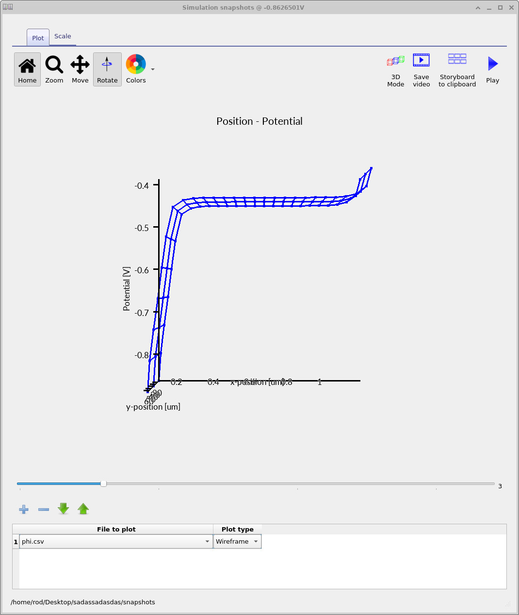
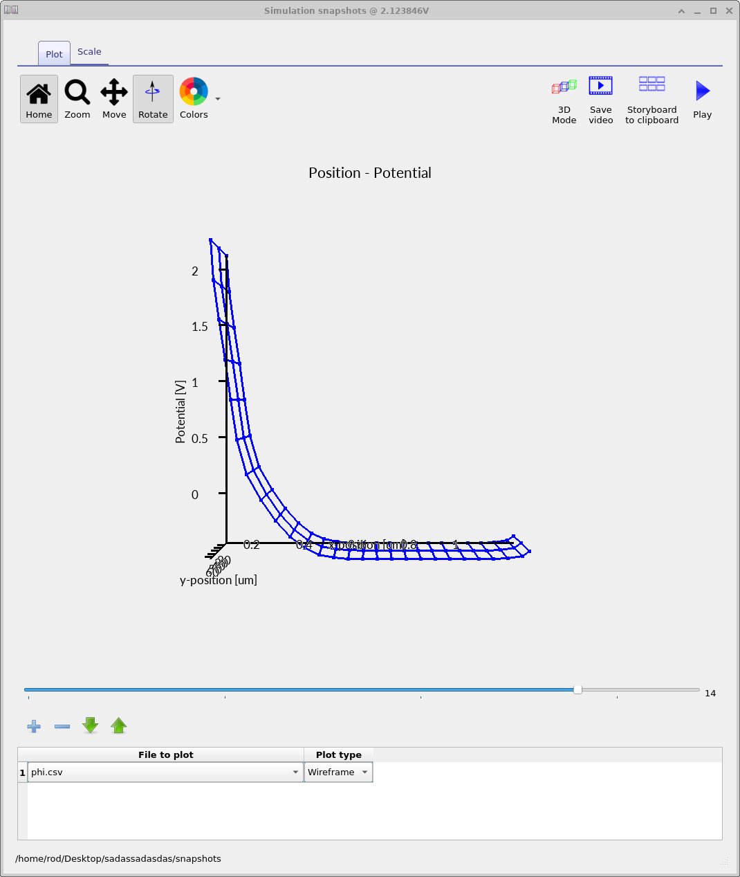
At negative gate bias, the potential varies sharply across the oxide but remains almost constant in the bulk silicon. This indicates that the p-type silicon can readily rearrange charge to screen the applied field, leaving only a weak electric field deep in the substrate. As the gate voltage becomes positive, the silicon can no longer fully screen the electric field. A pronounced potential gradient develops near the Si/SiO2 interface, defining a depletion region whose width increases with gate bias. This surface potential is the key quantity that will determine how the energy bands bend.
In the next section, we will examine the conduction and valence band edges. These band profiles do not introduce new physics; they are a direct consequence of the electrostatic potential distributions analysed here.
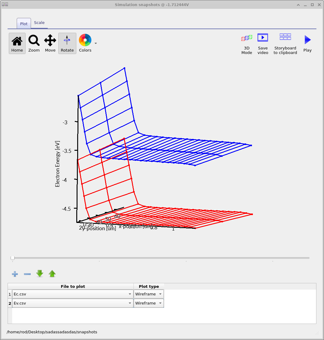
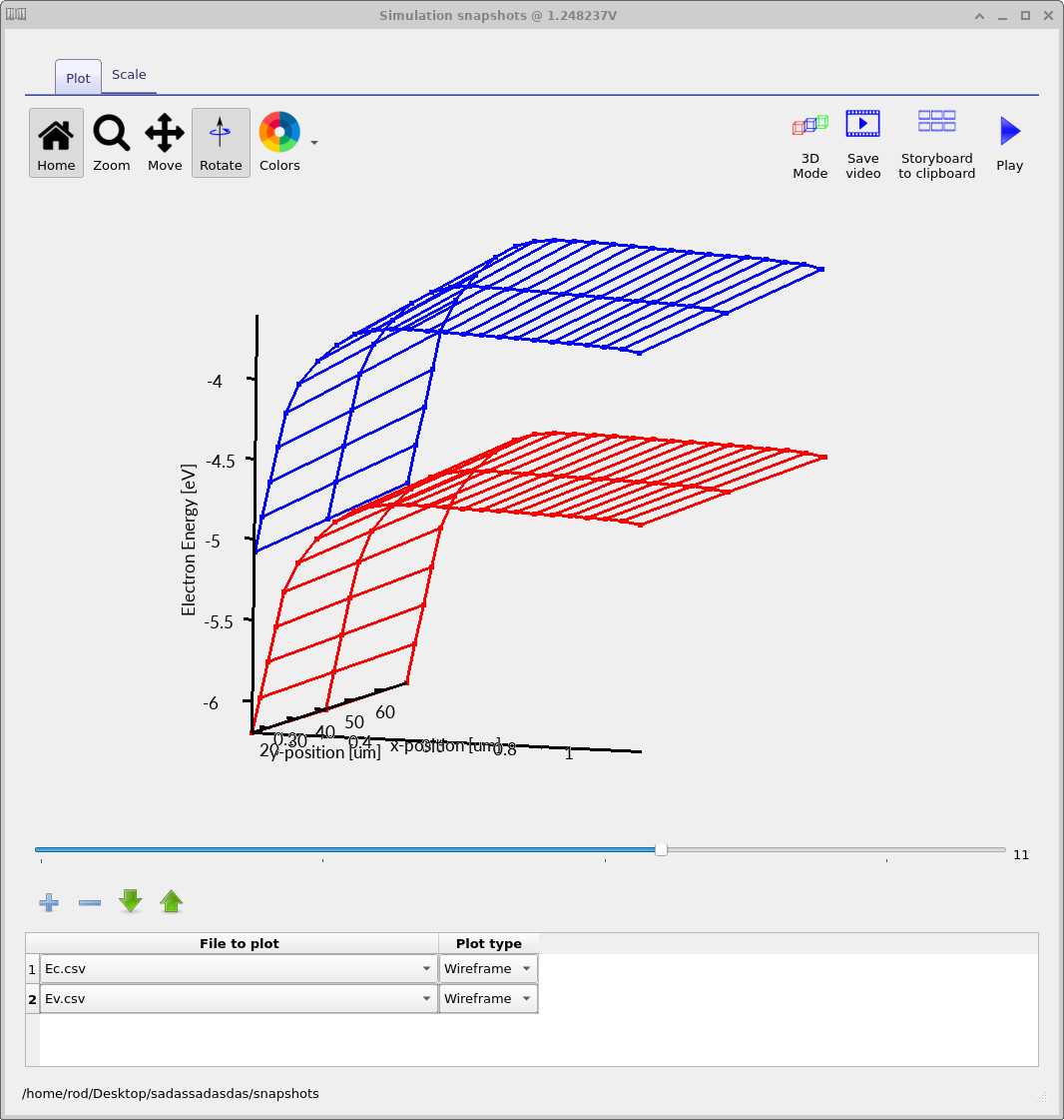
3. Conduction and valence band bending
We now examine the conduction band (Ec.csv) and valence band (Ev.csv)
as functions of position for different applied gate voltages.
Plotted together, these quantities provide a direct visualisation of
band bending in the silicon, which is the immediate consequence
of the electrostatic potential analysed in the previous section.
Before interpreting the plots, it is useful to recall how the band edges are defined.
In the drift–diffusion formulation used here, the conduction and valence band energies
are related to the electrostatic potential phi by
Ec(x) = −χ − q φ(x)
and
Ev(x) = −χ − Eg − q φ(x)
where χ is the electron affinity, Eg is the band gap,
and φ(x) is the electrostatic potential.
Because both band edges depend linearly on phi, any spatial variation in the
electrostatic potential appears directly as bending of the conduction and valence bands.
The band edges are visualised using the snapshots output.
Open the snapshots viewer from the Output tab as before, then click the
blue plus icon twice to add two plot entries.
Select Ec.csv for the first entry and Ev.csv for the second.
This allows the conduction and valence band edges to be viewed together in three dimensions
as functions of position and applied gate voltage.
At negative gate bias, both the conduction and valence bands bend upward near the Si/SiO2 interface. Since the band edges follow the electrostatic potential, this upward bending reflects an increase in surface potential relative to the bulk. From the band profiles alone, we can infer that the surface region is driven toward a hole-rich electrostatic configuration.
As the gate voltage becomes positive, the bands bend downward near the interface. This change in curvature indicates a reduction in surface potential and the formation of a depleted region in the silicon. At this stage the NMOS capacitor is electrostatically depleted but not yet inverted. No assumptions about carrier densities are required to reach this conclusion—the band bending directly encodes the underlying electrostatics.
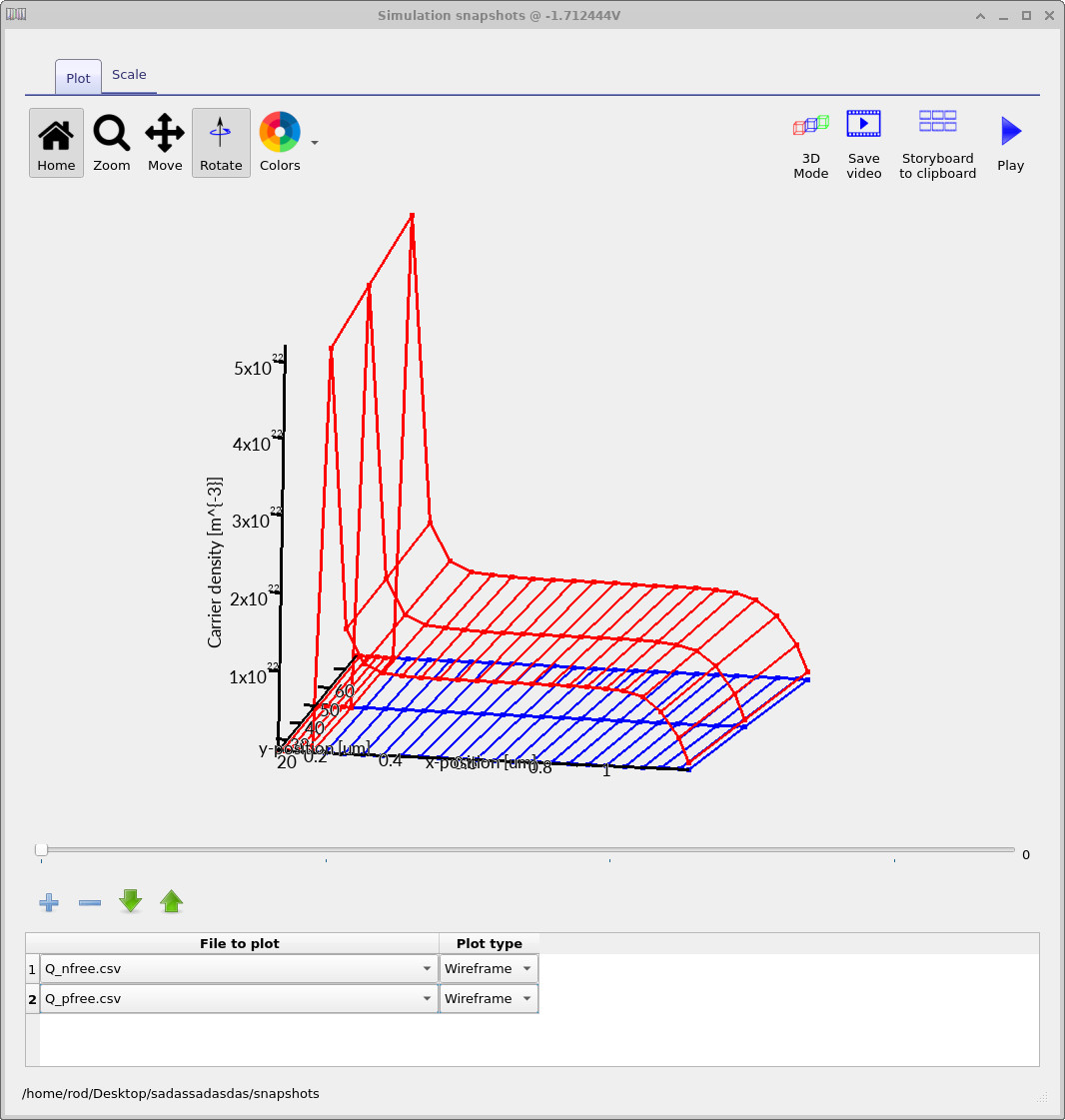
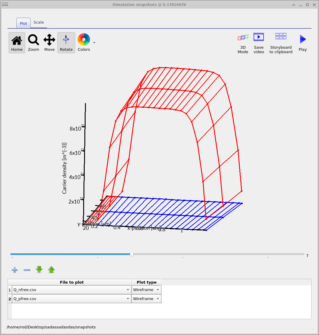
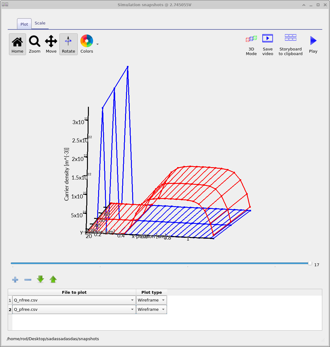
4. Free carrier densities
We now make the electrostatic response of the NMOS capacitor explicit by examining the
free carrier densities in the silicon.
Figure ??–
??
show the hole density (Q_pfree.csv) and electron density (Q_nfree.csv)
extracted from the snapshots output at representative gate voltages. In the snapshots viewer, the colour assignment is determined purely by plot order:
the first quantity added is rendered in blue, and the
second in red.
In the figures shown here, electrons (Q_nfree.csv) are plotted first and therefore
appear in blue, while holes (Q_pfree.csv) are plotted second and appear in red.
If these files are added in the opposite order, the colours will be reversed.
At negative gate bias (Fig. ??), the red surface corresponds to the hole density. A sharp increase is visible at the Si/SiO2 interface, indicating electrostatic accumulation of holes. The blue surface (electron density) remains negligible throughout the silicon, consistent with a p-type substrate under negative bias. As the gate bias is increased toward zero (Fig. ??), the red surface near the interface drops in magnitude. Holes are repelled from the surface, and a region of reduced mobile charge develops. This marks the onset of depletion, where the space charge is increasingly dominated by fixed ionised acceptors rather than free carriers.
Under positive gate bias (Fig. ??), the hole density (red) is strongly suppressed near the interface, defining a clear depletion region. The electron density (blue) remains low throughout this bias range, showing that the device has not yet entered strong inversion.
Taken together, these carrier-density plots provide a direct and quantitative confirmation of the electrostatic picture inferred earlier from the potential and band-edge diagrams. They show explicitly how accumulation and depletion arise from the redistribution of mobile charge in the silicon. The transition to strong inversion—where electrons dominate the surface charge—is deferred to later tutorials.
5. Fermi levels and band occupation
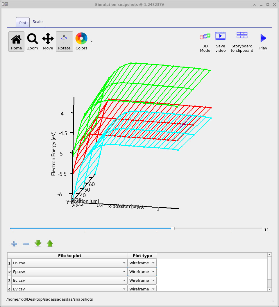
We now bring together the energy bands and carrier statistics by plotting the
conduction band (Ec.csv), valence band (Ev.csv), and the electron and hole
quasi-Fermi levels (Fn.csv and Fp.csv) from the snapshots output.
Taken together, these quantities describe not only the electrostatics of the NMOS capacitor,
but also how carriers occupy the available states under bias.
To reproduce the plot shown in
??,
open the Output tab, double-click the snapshots directory, and use the
blue plus icon to add four plot entries. Select, in order:
Fn.csv— electron quasi-Fermi levelFp.csv— hole quasi-Fermi levelEc.csv— conduction band edgeEv.csv— valence band edge
The snapshots viewer assigns colours based on plotting order: the first quantity is blue, the second red, and subsequent entries follow. In the figure shown here, the quasi-Fermi levels appear above the bands, with electrons and holes clearly distinguished by colour. If you change the order in which the files are added, the colours will change accordingly.
Use the slider at the bottom of the snapshots window to move through the voltage sweep. This allows you to track continuously how the band edges and quasi-Fermi levels evolve as a function of applied gate bias.
Physically, this behaviour is exactly what one expects for an NMOS capacitor. There is no source–drain path and no DC current flowing through the structure. As a result, the electron and hole quasi-Fermi levels remain very close to one another and nearly flat throughout the device. Any small separation that appears is a numerical artefact of finite bias stepping and does not represent sustained carrier transport.
The band bending observed earlier is therefore driven entirely by electrostatics: the gate voltage modifies the electrostatic potential, which shifts the band edges according to
Ec(x) = −q φ(x) − χ and Ev(x) = Ec(x) − Eg
where φ is the electrostatic potential, χ is the electron affinity, and Eg is the band gap. The quasi-Fermi levels simply indicate how these bands are occupied locally; in a purely electrostatic MOS capacitor, they do not diverge.
💡 What to take away:
Across this tutorial you have seen the same physics expressed in several complementary ways:
electrostatic potential, band bending, carrier densities, and Fermi levels.
All of them describe the same underlying process — redistribution of charge in response
to a gate-controlled electric field.
🧪 Try this yourself:
Using the same NMOS capacitor structure, explore how the electrostatics respond
to changes in material and bias parameters. In all cases, keep the device geometry fixed.
- Change the SiO2 permittivity and observe how the potential drop and band bending in the silicon change at the same gate voltage.
- Modify the substrate doping concentration and compare the depletion width and curvature of the band edges.
- Extend the gate-voltage sweep range and track how φ, Ec, Ev, and the carrier densities evolve together.
- Switch between Maxwell–Boltzmann and Fermi–Dirac statistics in the silicon layer and compare the carrier density near the interface.
Expected outcomes
- Increasing oxide permittivity strengthens capacitive coupling, shifting more of the applied voltage into the silicon.
- Heavier p-type doping produces a narrower depletion region; lighter doping produces wider depletion and smoother band bending.
- Extending the bias range increases band bending but does not, by itself, separate the quasi-Fermi levels in a capacitor geometry.
- Fermi–Dirac statistics suppress unphysical carrier overpopulation near the interface at high densities.