MOS Capacitor (NMOS): Electrostatics, Depletion & Band Bending
1. Introduction
A MOSFET (Metal–Oxide–Semiconductor Field-Effect Transistor) works by using a gate voltage to electrostatically control the carrier density at a semiconductor surface. The simplest “atom” of MOSFET physics is the MOS capacitor: a metal gate, an insulating oxide, and a doped semiconductor. If you understand the MOS capacitor, you understand the electrostatics that make a MOSFET switch (see ??).
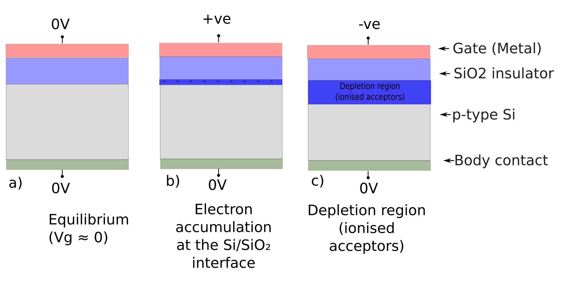
An NMOS device is called “NMOS” because, when biased on in a transistor geometry, it forms an n-type inversion channel—the conducting channel carriers are electrons. In practice this is commonly realised with a p-type silicon body (acceptor-doped Si) and a sufficiently positive gate bias. Even before you introduce source and drain, the same gate electrostatics is visible in the MOS capacitor: a positive gate bias draws electrons towards the Si/SiO2 interface (surface accumulation), while a negative gate bias repels holes and leaves behind a region of fixed ionised acceptors (depletion), as illustrated in ??.
A PMOS device is the complementary case: it forms a p-type channel (holes as the conducting carriers), commonly using an n-type body under negative gate bias. NMOS/PMOS together form the basic complementary pair used in CMOS logic.
In this tutorial we build and explore a 2D NMOS capacitor structure in OghmaNano. We focus deliberately on the accumulation and depletion regimes, where the physics is dominated by electrostatics and the results are easy to interpret. Strong inversion (a true conducting channel) is deferred to Part B and later tutorials.
2. Launch OghmaNano
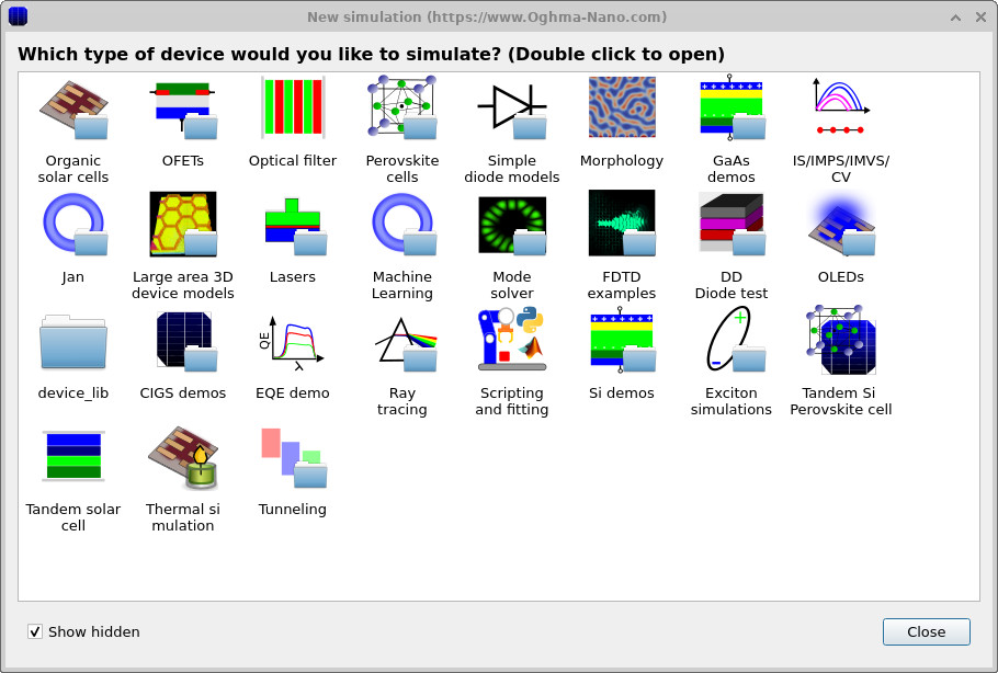
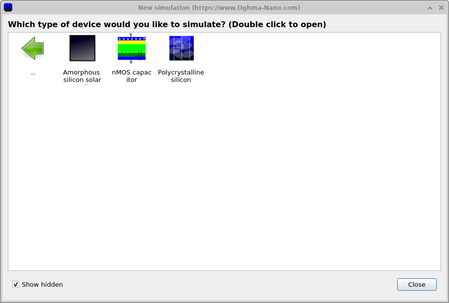
Start OghmaNano from the Windows Start menu. The main OghmaNano window will appear as shown in ??. Click New simulation. This opens the library of available device types, shown in ??. Double-click Si demos to open the silicon example set, then select the nMOS capacitor example as shown in ??. When prompted, save the simulation to a local folder with write access. After saving, the main simulation window opens (see ??).
💡 Tip: Save simulations to a local drive (e.g. C:\) for best performance.
Network or cloud-backed folders can slow repeated solver runs.
3. Inspect the device structure (layers and materials)
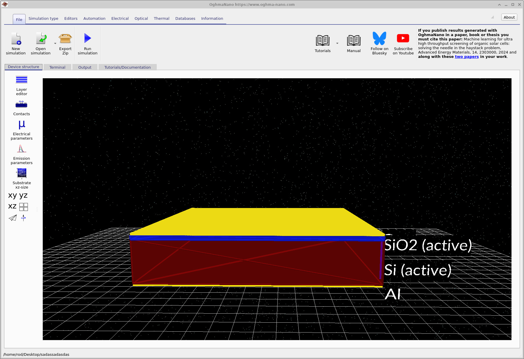
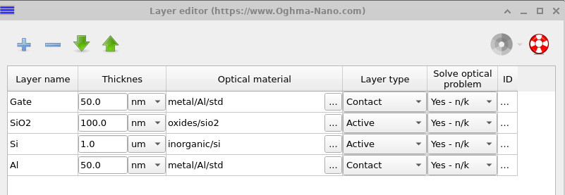
After creating the project, the main simulation window opens showing a deliberately simplified NMOS MOS capacitor structure: a metal gate, a SiO2 gate oxide, and a p-type silicon substrate with a body contact. It is referred to as an NMOS capacitor because the semiconductor body is p-type, and a positive gate bias drives the surface electrostatics toward electron accumulation. This structure represents the canonical NMOS electrostatic configuration and is widely used to study band bending, accumulation, and depletion at the Si/SiO2 interface.
In practical devices the MOS capacitor is often embedded within more complex layouts or combined with additional contacts. Here, those elements are intentionally omitted so that the focus remains entirely on the vertical electrostatics of the NMOS capacitor itself. By removing lateral transport and geometric complexity, the physical origin of charge redistribution and electrostatic potential variation in the semiconductor can be examined directly and without ambiguity.
The layer structure can be inspected in the Layer editor. For clarity, the oxide thickness in this tutorial is chosen to be slightly larger than in modern silicon technology, so that the resulting potential drop, accumulation layer, and depletion region are clearly visible in the output plots. In contemporary NMOS capacitors, oxide thicknesses are typically on the order of 10 nm or below. After completing the tutorial, you are encouraged to adjust the layer thicknesses and explore how the electrostatic response changes as the structure approaches realistic device dimensions.
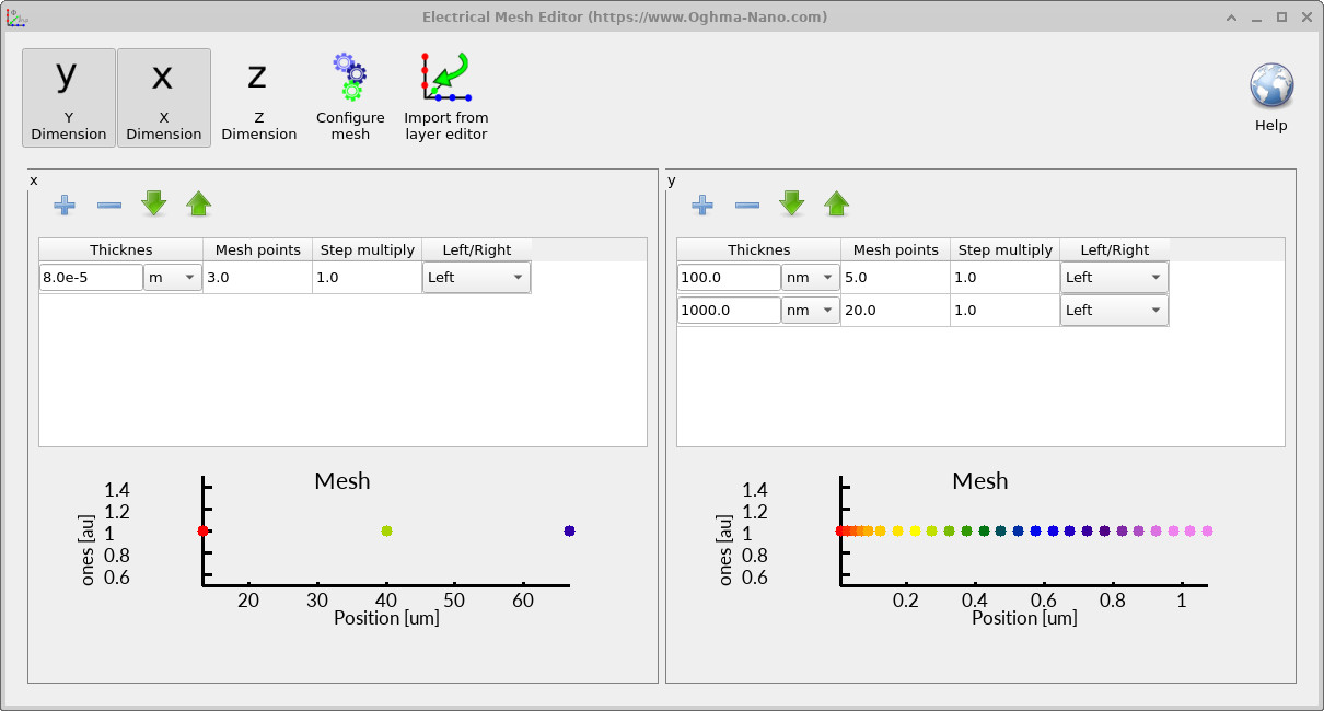
4. Inspect the electrical ribbon and 2D mesh
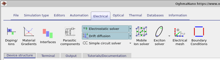
Most of the NMOS capacitor workflow lives in the Electrical ribbon. From here you can choose which electrical model is active, edit parameters, inspect doping, and configure the mesh. Clicking Electrical mesh opens the mesh editor (see ??).
This tutorial uses a 2D mesh: the device is resolved in two dimensions to capture band bending and depletion near the interface while keeping runtimes short. In the example shown, there are only a few points along one direction (lateral) and a denser sampling through the oxide and silicon thickness (vertical), where the electrostatic gradients live. You can increase the number of mesh points, but the computational cost rises roughly with the number of unknowns (and, for nonlinear problems, the number of iterations per bias point).
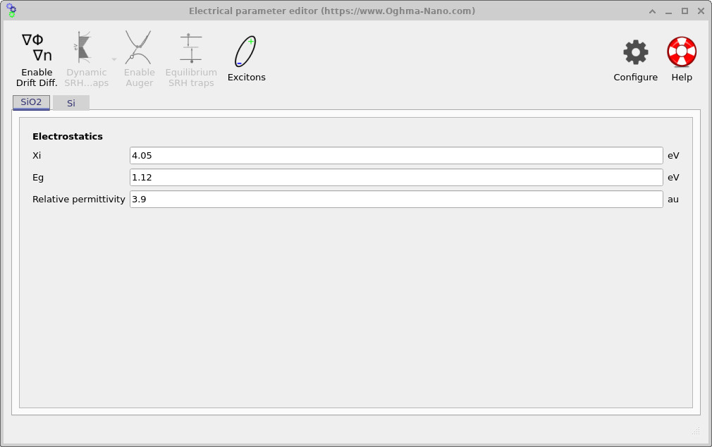
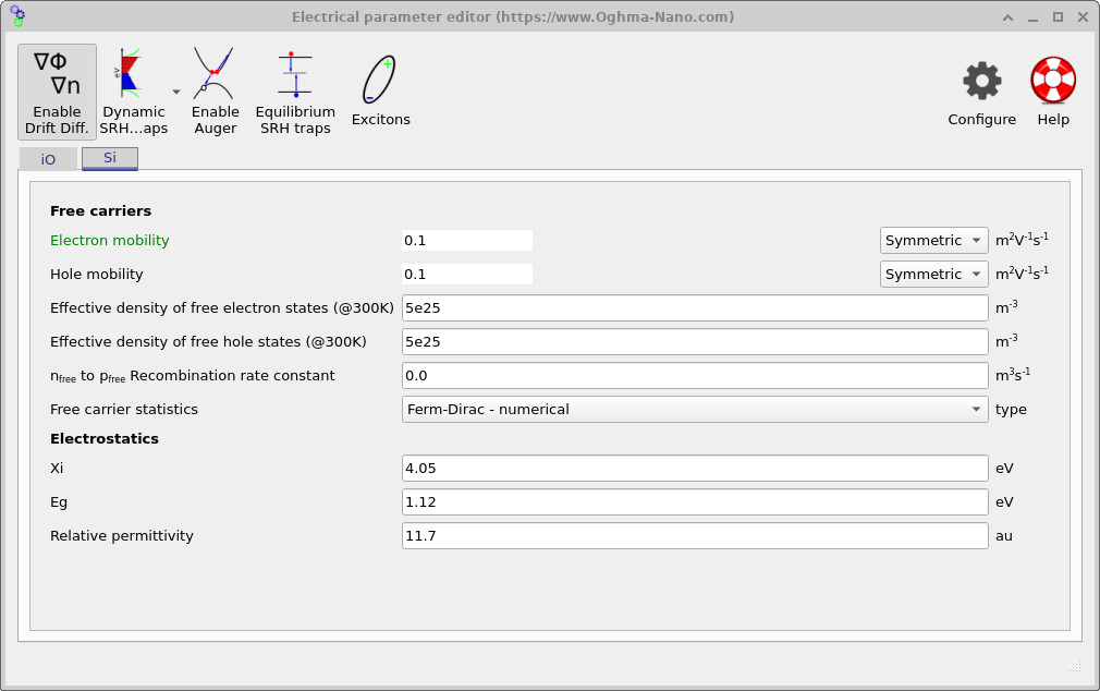
5. Electrical Parameter Editor (oxide vs silicon)
Clicking Electrical parameters opens the Electrical Parameter Editor. This editor is organised by material: the SiO2 tab contains oxide parameters, while the Si tab contains silicon parameters. For the silicon layer, we use a physically sensible parameter set: a relative permittivity of approximately 11.7, standard silicon values for the electron affinity and band gap, finite electron and hole mobilities, and realistic effective densities of states. Importantly, we select Fermi–Dirac statistics rather than Maxwell–Boltzmann statistics, since under gate bias the carrier density near the Si/SiO2 interface can become high enough that degeneracy effects are important.
For the oxide layer, by contrast, the only parameter that plays a central role in this tutorial is the relative permittivity. The SiO2 is treated as an ideal insulator: it supports an electric field and a voltage drop, but it does not support mobile charge. As a result, the electrostatic behaviour of the NMOS capacitor is governed by how the applied gate voltage divides between the oxide and the silicon, which is set entirely by the oxide thickness and permittivity.
This modelling choice is reflected in the buttons at the top of the editor. In the SiO2 layer, drift–diffusion is disabled, so only Poisson’s equation is solved there. In contrast, in the silicon layer, drift–diffusion is enabled so that the redistribution of electrons and holes in response to the gate bias can be captured correctly. This separation mirrors the physical roles of the two materials in an NMOS capacitor: the oxide mediates the electric field, while the silicon hosts the mobile carriers.
You may notice that parameters such as the electron affinity and band gap listed for SiO2 appear similar to those of silicon. In the context of this tutorial, that is intentional and benign. Because carrier transport equations are not solved in the oxide, these band parameters do not influence the solution: there is no mechanism for electrons or holes to enter the oxide in the model. The SiO2 therefore participates only through its dielectric response, not through its electronic band structure.
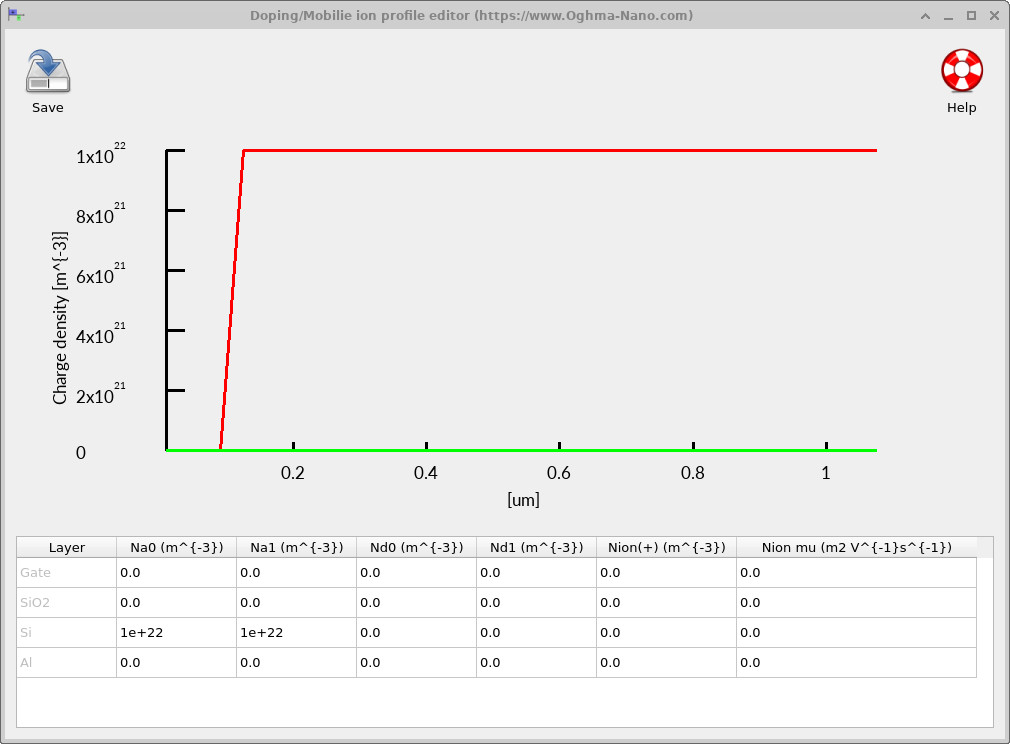
6. Doping editor (substrate doping profile)
Finally, open the Doping editor from the Electrical ribbon to inspect the dopant distribution (see ??). For an NMOS capacitor, the silicon substrate is typically p-type (acceptor-doped). At zero or negative gate bias, holes are the majority carriers near the Si/SiO2 interface. As the gate bias becomes positive, the gate electric field repels holes from the surface, leaving behind ionised acceptors (fixed negative charge) and forming a depletion region.
The dopant concentration strongly controls the electrostatic response of the capacitor. Heavier p-type doping results in a thinner depletion region for a given surface potential, while lighter doping produces a wider depletion region and a larger spatial extent of band bending. In Part B we will use this editor to deliberately modify the substrate doping and observe the resulting changes in depletion width, electrostatic potential, and band structure.
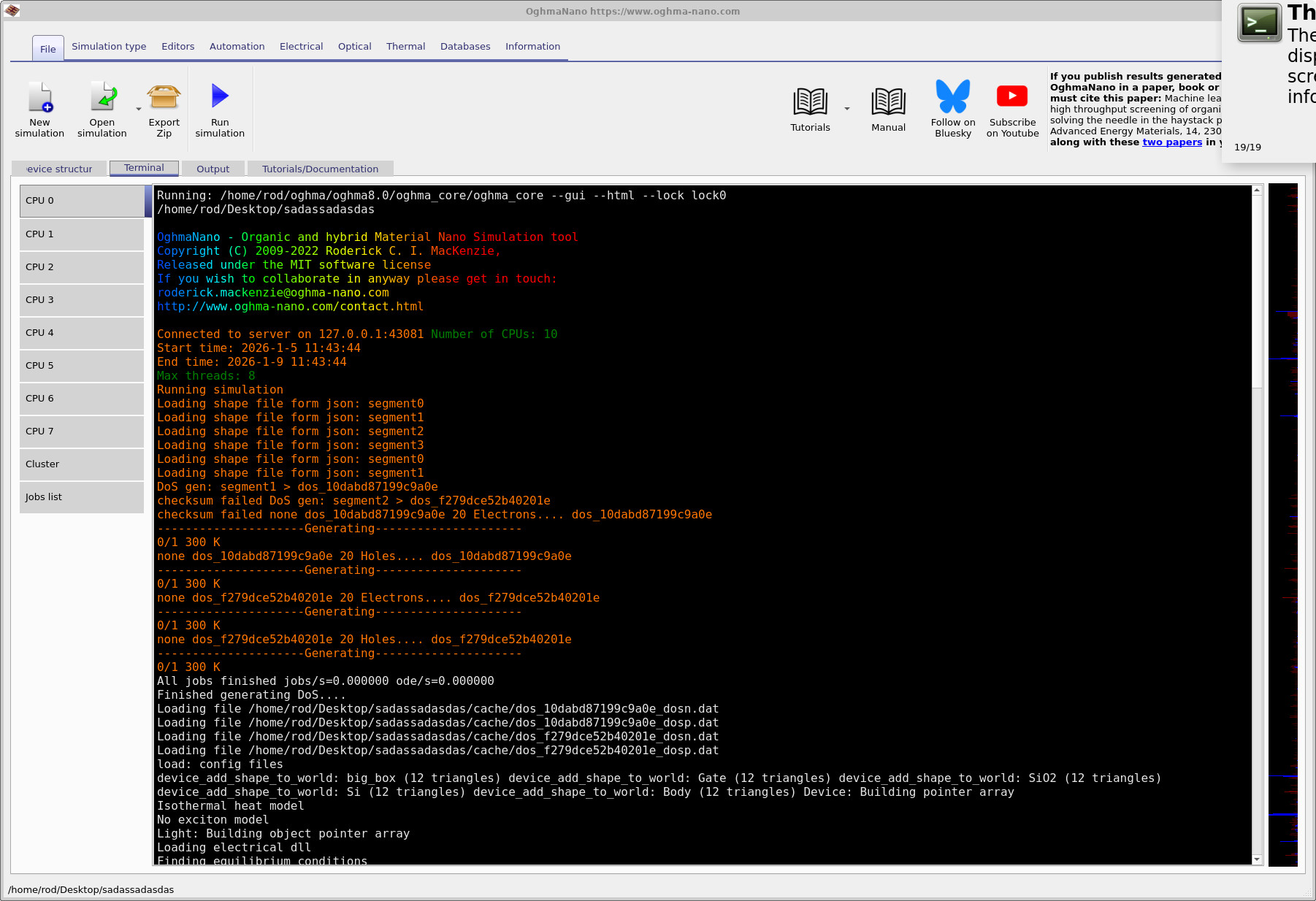
7. Run the simulation (Terminal output)
Click Run simulation (the blue arrow) in the main window. OghmaNano will switch to the Terminal tab and begin running the solver. The first stage of a typical run is shown in ??, there you can see the command line used to launch the core solver, followed by project loading and model initialization. The repeated Generating... lines indicate that OghmaNano is building lookup tables for Fermi–Dirac statistics (for electrons and holes in the layers you selected). Evaluating Fermi–Dirac integrals accurately is expensive, so the code tabulates these quantities once, then reuses them during the nonlinear iterations. When you see Loading file, it is reloading the cached tables (or other cached intermediate data) to avoid regenerating them on every run.
A second key stage is bias ramping. Before the main sweep begins, the solver gradually ramps the gate from a known, easy starting point (typically near equilibrium) to the first bias point requested (here, to -2 V). This is a continuation strategy: Newton-type solvers converge reliably only when the initial guess is reasonably close to the solution. Jumping straight to a large bias can put the initial guess “too far away”, causing divergence or slow, unstable convergence. By stepping the gate voltage in small increments, each solution provides a good initial guess for the next.
Once the gate has reached the start voltage, the solver proceeds with the gate sweep (the “J–V”/bias curve). The device body is held at 0 V (as reported in the terminal). You may notice the printed current density fluctuates in sign and magnitude even though a capacitor should have (essentially) zero steady-state DC current. That behaviour is normal here: the solver is reporting very small residual currents near the numerical noise floor of the nonlinear solve. In other words, the “spikiness” is not a physical DC current; it is a symptom of trying to compute a quantity that is truly ~0 to high relative accuracy.
The quantity reported as f(...)= is the nonlinear residual/error measure (a convergence metric). When this value is very small,
the electrostatic solution (potential, charge, band bending) is considered converged. The time shown at the right (in milliseconds) is the
runtime per bias step / iteration block, and is useful for profiling and for judging the cost of increasing mesh density.
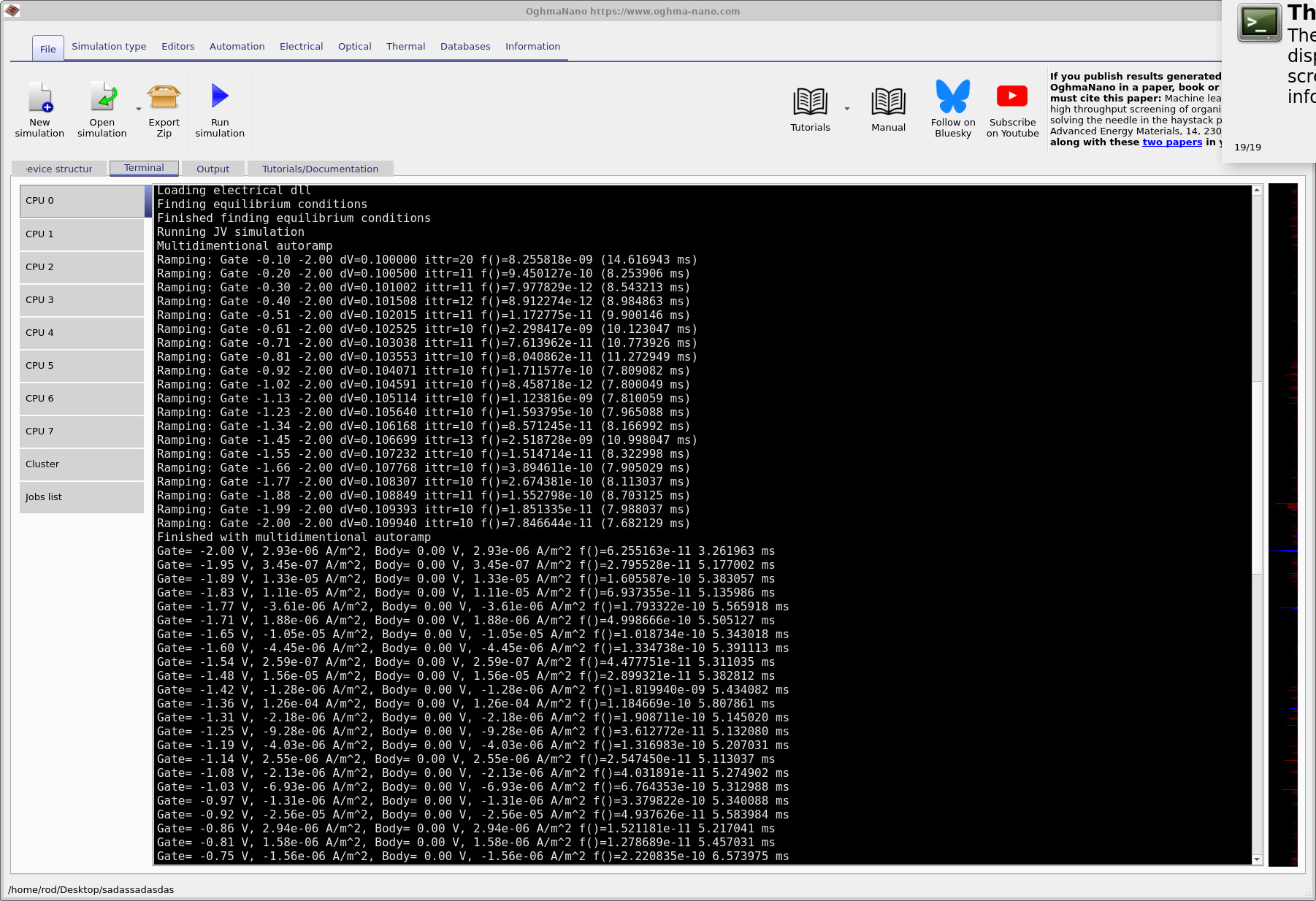
f(...) value is the solver residual (convergence metric).
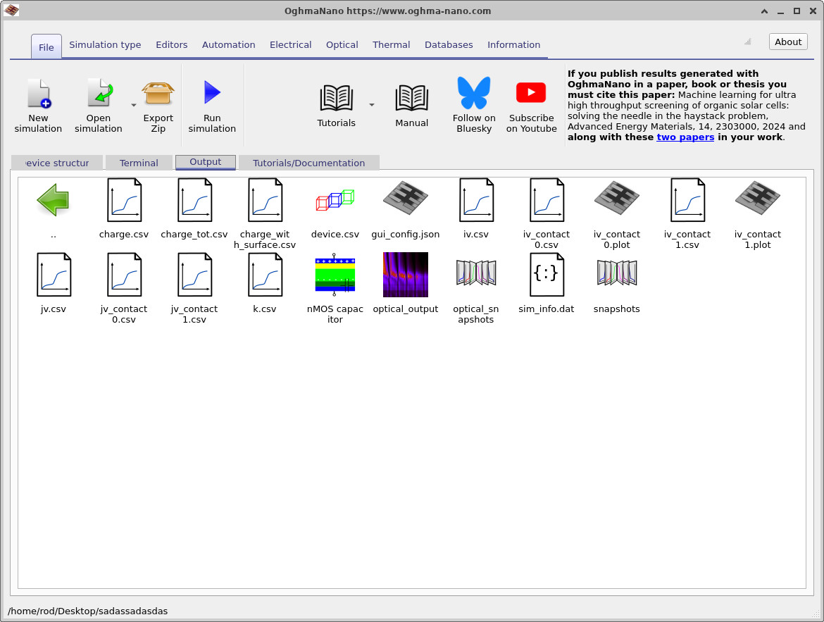
8. Output files and contact current
When the run completes, switch to the Output tab to view the files produced by the simulation
(see ??).
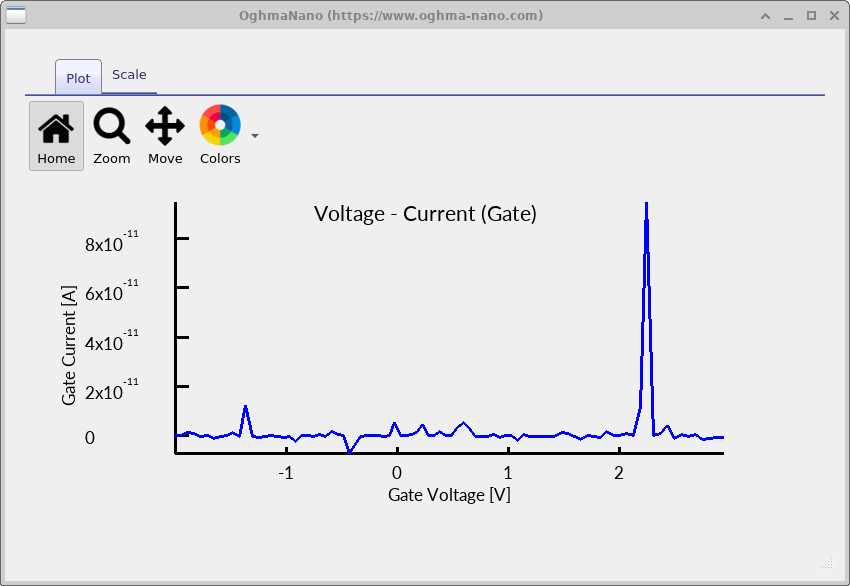
You can double-click entries such as iv_contact_0.csv and iv_contact_1.csv to open the contact current plots.
For an ideal MOS capacitor, the steady-state DC current is essentially zero, since the structure is purely electrostatic. The contact current plots are therefore included mainly for background and completeness, and as a simple sanity check that no unintended current paths are present. The curves should remain close to zero across the bias sweep; small fluctuations are normal and simply reflect the fact that the true current is vanishingly small.
In the next section we will move beyond these auxiliary outputs and focus on the physically meaningful results of the simulation: the electrostatic potential, band edges, Fermi levels, and carrier distributions within the NMOS capacitor.
💡 What you’ve learned so far: In this tutorial you set up and inspected an NMOS capacitor simulation (device structure, mesh, material parameters, and doping). In Part B we build on this by applying gate bias and interpreting the simulation output—band bending, electrostatic potential, carrier densities, and surface depletion.