GaAs Tutorial (Part A): Run a 3D Drift–Diffusion Simulation with a Vertical Defect
1. Introduction
In this tutorial you’ll run a 3D drift–diffusion simulation of a GaAs pn diode containing an intentionally obvious vertical defect (a top-to-bottom shunt through the stack). This is a deliberately “unfair” problem for 1D models: the defect forces lateral current flow, current crowding, and localised recombination that cannot exist in a purely through-thickness simulation. Why this matters: in real devices, performance is often limited not by the ideal layer stack but by where the current actually flows. Local defects, pinholes, edge leakage, finite contacts, and non-uniform materials can dominate the measured JV. A 3D drift–diffusion model lets you link features in the JV curve directly to specific regions of the device, answering questions that 1D cannot.
How to use this in your own work: treat the defect here as a template for any localised non-ideality—for example a shunt filament,
a pinhole through a blocking layer, a grain boundary, a damaged probe region, or a finite-area electrode.
The workflow is the same: build a minimal 3D geometry, keep the lateral mesh as small as possible, run the solver,
then use contact-resolved JV curves and snapshots (jn.csv, \(\phi\), recombination) to connect electrical behaviour to physical location.
The goal is twofold: (1) give you a practical entry point to genuinely 3D electrical modelling in OghmaNano, and (2) teach the modelling decision: when 3D is essential (defects, finite contacts, lateral variation) and when it collapses to 1D. In Part A you run the defective device, in Part B you remove the defect and show that 3D/2D/1D agree once symmetry is restored, and in Part C you enable illumination and see where numerical sensitivity appears at low current.
2. Getting started
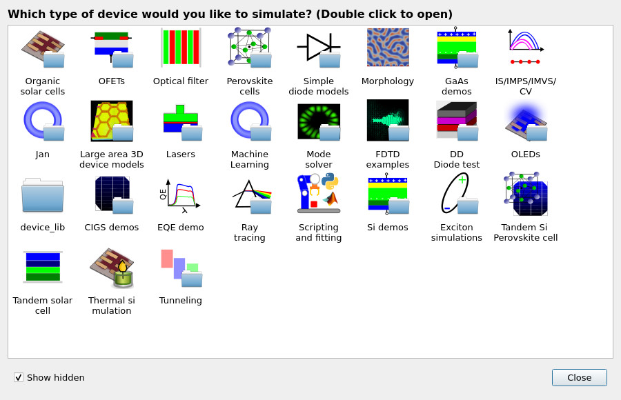
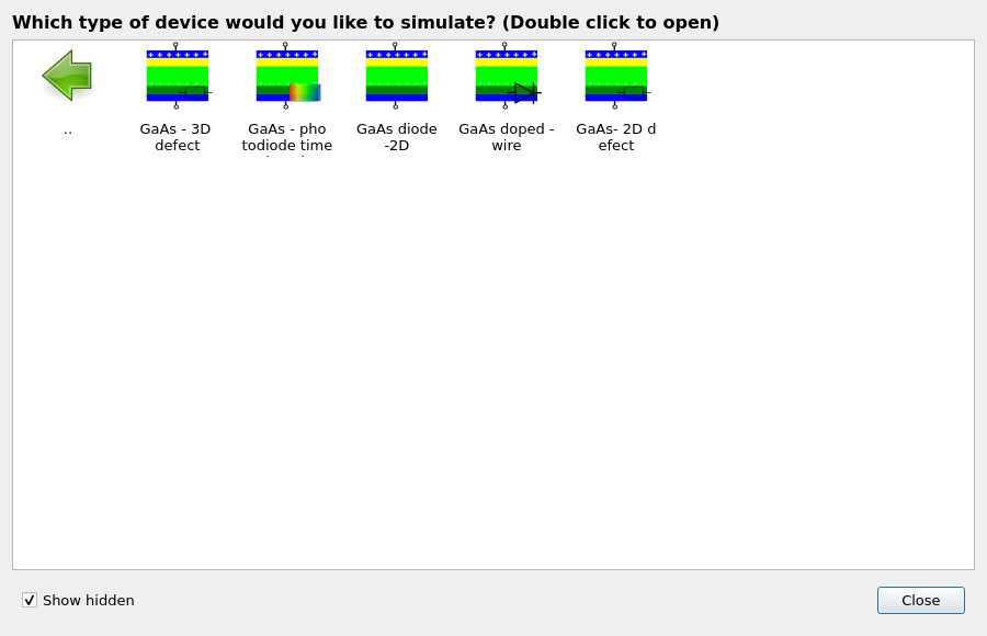
From the main OghmaNano window, click New simulation to open the device library (see ??). Double-click GaAs demos. This opens a folder of gallium arsenide examples (see ??). Finally, double-click GaAs - 3D defect and save the simulation to a folder you have write access to.
💡 Tip: For best performance save to a local drive. Simulations stored on network, USB, or cloud folders (e.g. OneDrive) can run slowly due to heavy read/writes.
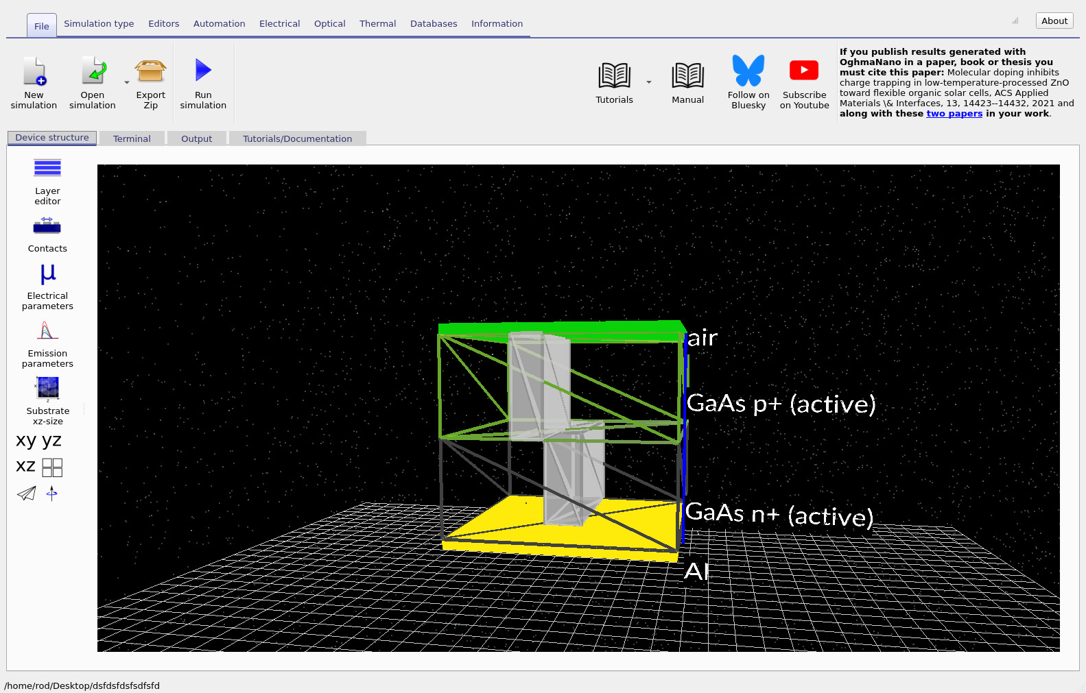
After opening the example, the main window shows a 3D view of the device (see ??). The structure is a GaAs pn diode containing two visible blocks that represent an intentional vertical defect region (for example, an impurity filament or short-circuit-like loss path). The defect runs from top to bottom through the device, making it intrinsically three-dimensional and capable of producing current crowding and spatially localised recombination that would be absent in a purely 1D model.
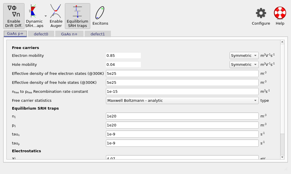
To inspect the material and defect parameters, go to the Device structure tab and click Electrical parameters to open the parameter editor (see ??). You will find separate parameter sets for:
- GaAs p+ and GaAs n+ (the diode layers), and
- defect0 and defect1 (the defect regions).
The example uses physically reasonable GaAs-like mobilities and carrier densities. Recombination includes a simple bimolecular free-to-free channel (often referred to in organic-device contexts as n3–p3) with a representative coefficient of 1 × 10⁻¹⁵ m3s−1.
You will also notice that equilibrium Shockley–Read–Hall (SRH) traps are enabled. In many organic-device simulations, dynamic SRH traps are required because trap occupancy stores significant charge and feeds back into the electrostatics. For GaAs, however, trap densities are typically low enough that traps can often be treated purely as a recombination loss mechanism. Using equilibrium SRH captures this physics without introducing additional state variables for stored trap charge, keeping the model both stable and efficient.
3. Exploring the simulation: doping and mesh
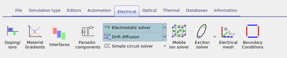
The Electrical ribbon provides access to the core electrical editors used to define and diagnose the simulation (see ??). In this section we will focus on two tools: Doping/Ions, which defines the pn junction, and Electrical mesh, which controls the spatial resolution of the drift–diffusion solve.
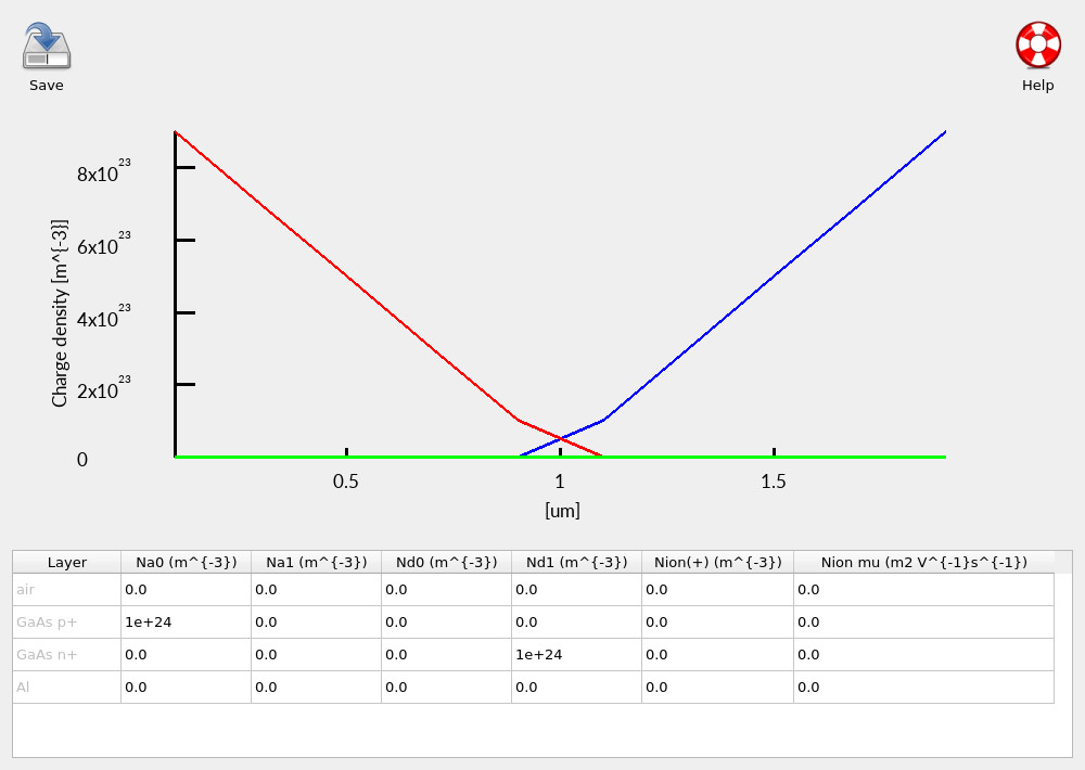
Click Doping/Ions to open the doping editor (see ??). This example is a deliberately simple pn diode, with clearly separated p-type and n-type regions. Keeping the doping profile simple here makes it easier to attribute any unusual behaviour later to geometry (the defect) rather than to electrostatics.
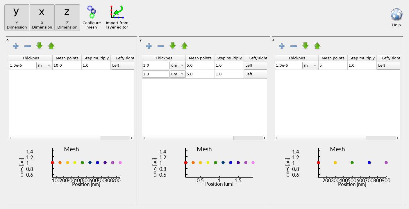
Next, click Electrical mesh to open the mesh editor (see ??). You will see that x, y, and z are all enabled, meaning the simulation is genuinely three-dimensional. In this coordinate system:
- y is the primary transport direction (through the diode thickness),
- x and z are lateral directions used to resolve the defect and lateral current flow.
The mesh in the y-direction is deliberately split across the n-type and p-type layers so that each region maintains an appropriate resolution—this becomes important if you later change layer thicknesses or introduce asymmetry. In contrast, the lateral meshes (x and z) use relatively few points (for example, ~10 in x and ~5 in z). This is intentional: in 3D, computational cost grows rapidly. If you increase the mesh density in each dimension by a factor \(k\), the total number of unknowns scales roughly as \(k^3\). In practical terms, 3D simulations become cubically slower as you refine the mesh, so you should keep lateral resolution as low as possible while still resolving the physics you care about.
4. Running the 3D simulation and viewing the results
To run the simulation, click Run simulation (the blue triangle). Because this is a genuinely three-dimensional drift–diffusion problem, it will take longer than a 1D run. On a reasonably modern laptop, the example should complete in roughly 30 seconds. If the runtime is significantly longer, first check that the simulation is saved to a local drive; network-mounted or cloud-synchronised folders can slow execution substantially due to heavy file I/O. Once the run finishes, open the Output tab (see ??). This directory contains the standard output files generated by a drift–diffusion solve, including snapshots of internal variables and current–voltage data. At this point it is important to distinguish between aggregate and contact-resolved outputs.
Because this device is simulated in 3D with finite-area contacts, you should generally
ignore the global jv.csv file and instead use the
contact-resolved JV curves.
The files jv_contact0.csv and jv_contact1.csv report the current associated
with the top and bottom contacts respectively.
In multidimensional simulations, these curves are the most physically meaningful way to interpret
electrical behaviour and to diagnose contact-specific losses. Open jv_contact0.csv to view the JV curve for the top contact
(see ??).
Because the device contains a vertical defect, this curve is not expected to resemble an ideal
1D pn-diode characteristic.
In the next section (Part B), you will disable the defect and see how the JV response changes—and
how the same structure collapses back to 2D and 1D once the intrinsic three-dimensional asymmetry
is removed.
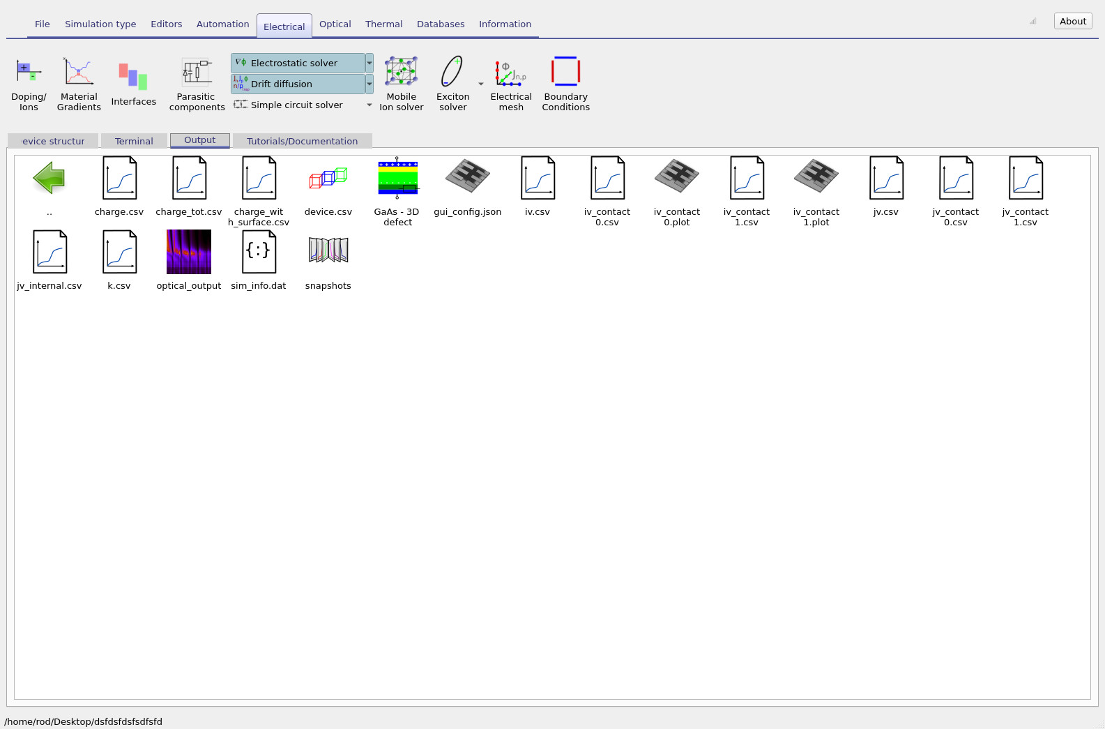
jv_contact0.csv and jv_contact1.csv over the aggregate jv.csv.
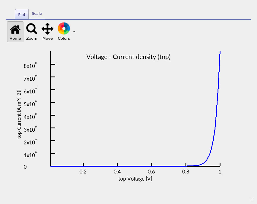
jv_contact0.csv curve (top contact) for the 3D GaAs diode containing the vertical defect.
5. Exploring internal variables with the snapshots viewer
To inspect what the solver is doing internally, open the snapshots/ directory in the output folder.
This gives access to spatially resolved simulator variables as a function of simulation step
(typically the applied bias).
Double-clicking the directory opens the snapshots viewer shown in
?? and
??.
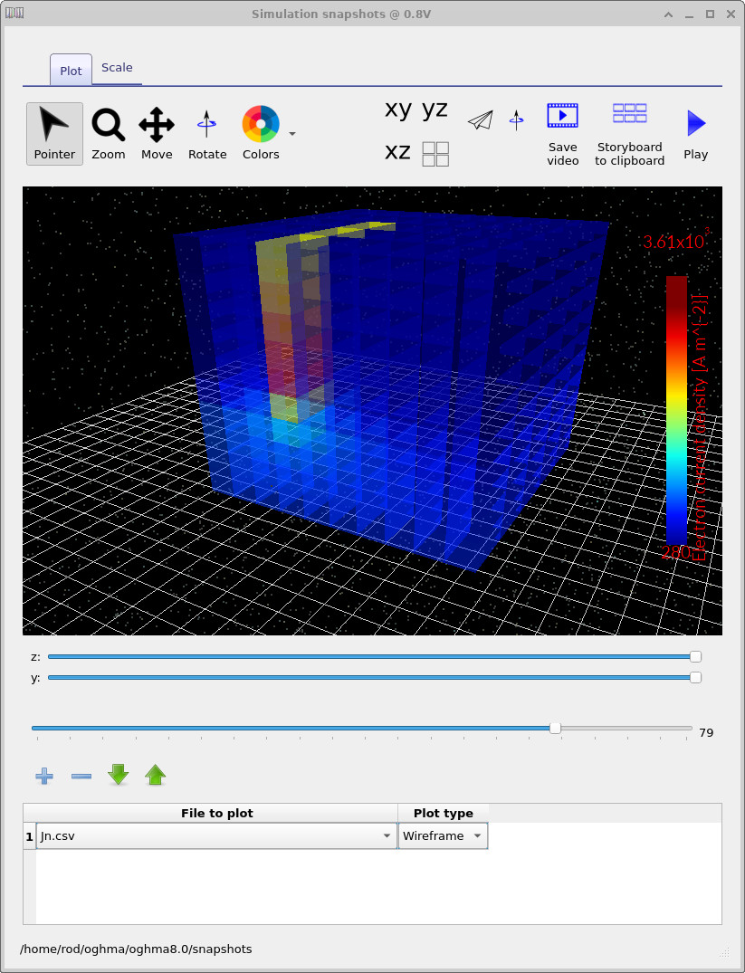
In the snapshots window, click the blue + button to add a plot and select
jn.csv from the File to plot drop-down menu.
The file jn.csv corresponds to the vertical electron current density.
Using the main slider, you can explore how the current distribution evolves with applied voltage,
while the y and z sliders allow you to take slices through the 3D volume.
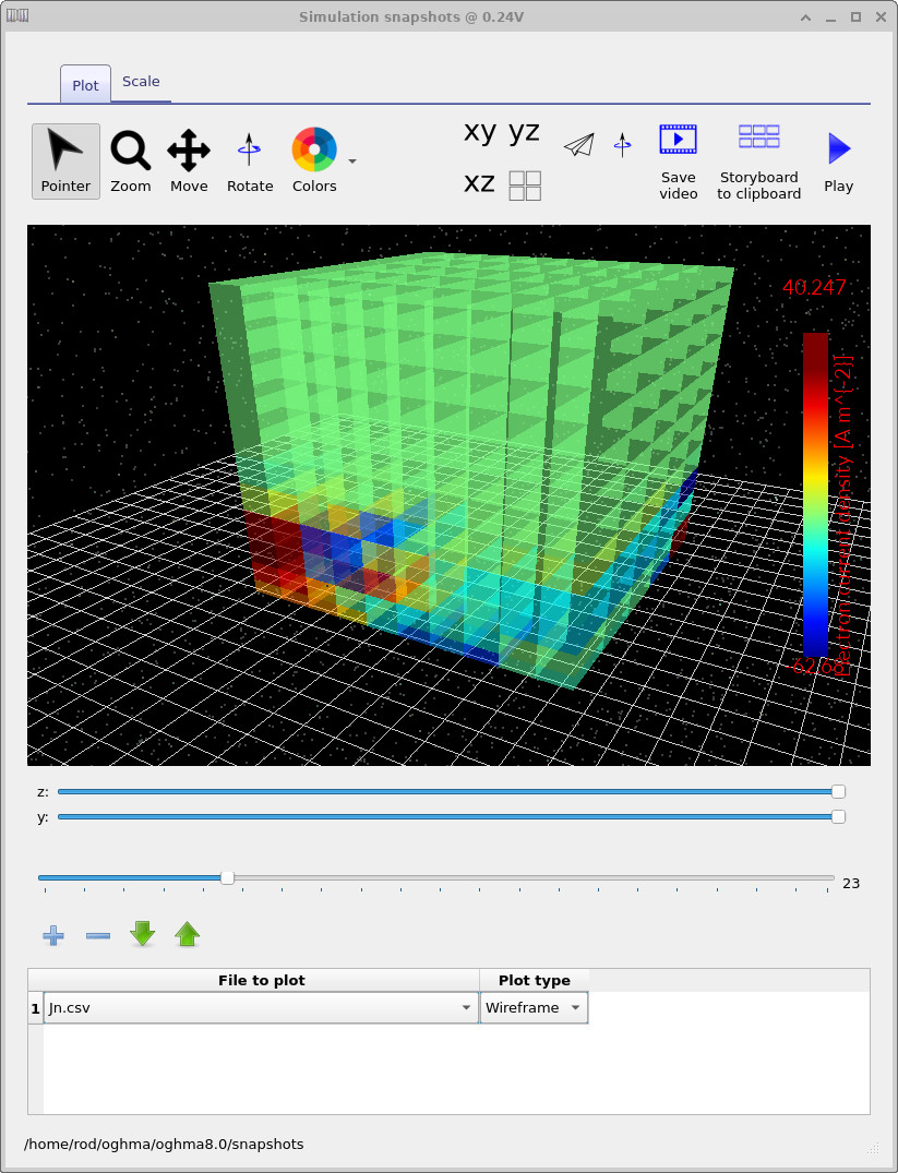
jn.csv at low applied voltage. The true current is close to zero, so the visible structure is dominated by numerical noise.
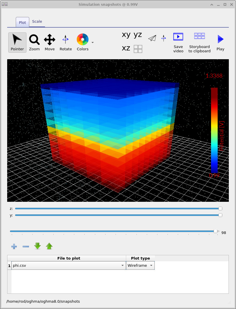
phi.csv: the electrostatic potential \(\phi\), showing how the internal potential redistributes with bias.
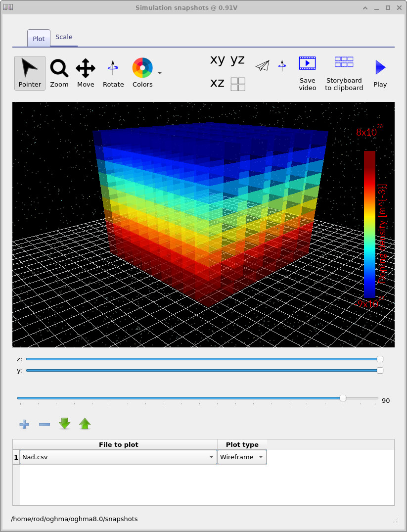
Nad.csv: the combined acceptor–donor doping distribution, fixed by the doping editor.
This example is a diode in the dark, so all current flow is electrically driven rather than photocurrent.
The key observation is that the defect produces a highly localised conduction path,
which can be visualised directly in 3D and linked unambiguously to the non-ideal JV behaviour. The snapshots viewer can be used to explore many other internal quantities, including Ec.csv and Ev.csv (band edges), quasi-Fermi levels, recombination rates, and carrier densities.
Exploring these fields alongside the JV curve is one of the most effective ways to build intuition
for how drift–diffusion solvers behave in multidimensional devices.
Note that while the electrostatic potential \(\phi\) evolves with applied bias,
the doping distribution (Nad.csv) is fixed by the doping editor and
does not change with voltage.
Even so, visualising doping in 3D is useful—particularly for later tutorials involving
lateral doping variations or spatially localised defects.
👉 Next step: Continue to Part B to remove the defect and compare the JV curves, or return to the silicon & semiconductor device overview.