GaAs Tutorial (Part B): 3D → 2D → 1D (Removing the defect)
1. Introduction: choosing between 3D, 2D and 1D drift–diffusion
A key modelling decision in semiconductor device simulation is choosing the appropriate dimensionality: 3D, 2D, or 1D. Higher-dimensional models are more expensive to run, but lower-dimensional models can miss important physics if lateral effects are present. This section focuses on learning when higher dimensionality is actually required. In Part A, the GaAs diode contained a vertical defect that forced lateral current flow, making the problem intrinsically 3D. Here, we remove that asymmetry by disabling the defect, turning the same device into a uniform structure that can be solved in 3D, 2D, and 1D using the same physical parameters.
As a rule of thumb, 1D models apply to laterally uniform stacks (e.g. ideal pn diodes or solar cells), 2D models capture a single lateral variation (e.g. OFETs, edge effects, or line defects), and 3D models are required for localised features such as shunts, filaments, finite-area contacts, or point defects. In this tutorial you will learn how to compare 3D, 2D and 1D drift–diffusion simulations, evaluate runtime and mesh scaling, and decide when higher-dimensional modelling adds real physical insight—and when it does not.
2. Remove the lateral asymmetry (disable the defect objects)
In Part A, the vertical defect forced lateral current flow and made the device intrinsically three-dimensional. To study how dimensionality alone affects runtime and results, we now remove this source of lateral variation while keeping the underlying geometry intact. Rather than deleting the defect, we will disable it so that the device becomes laterally uniform in the x and z directions.
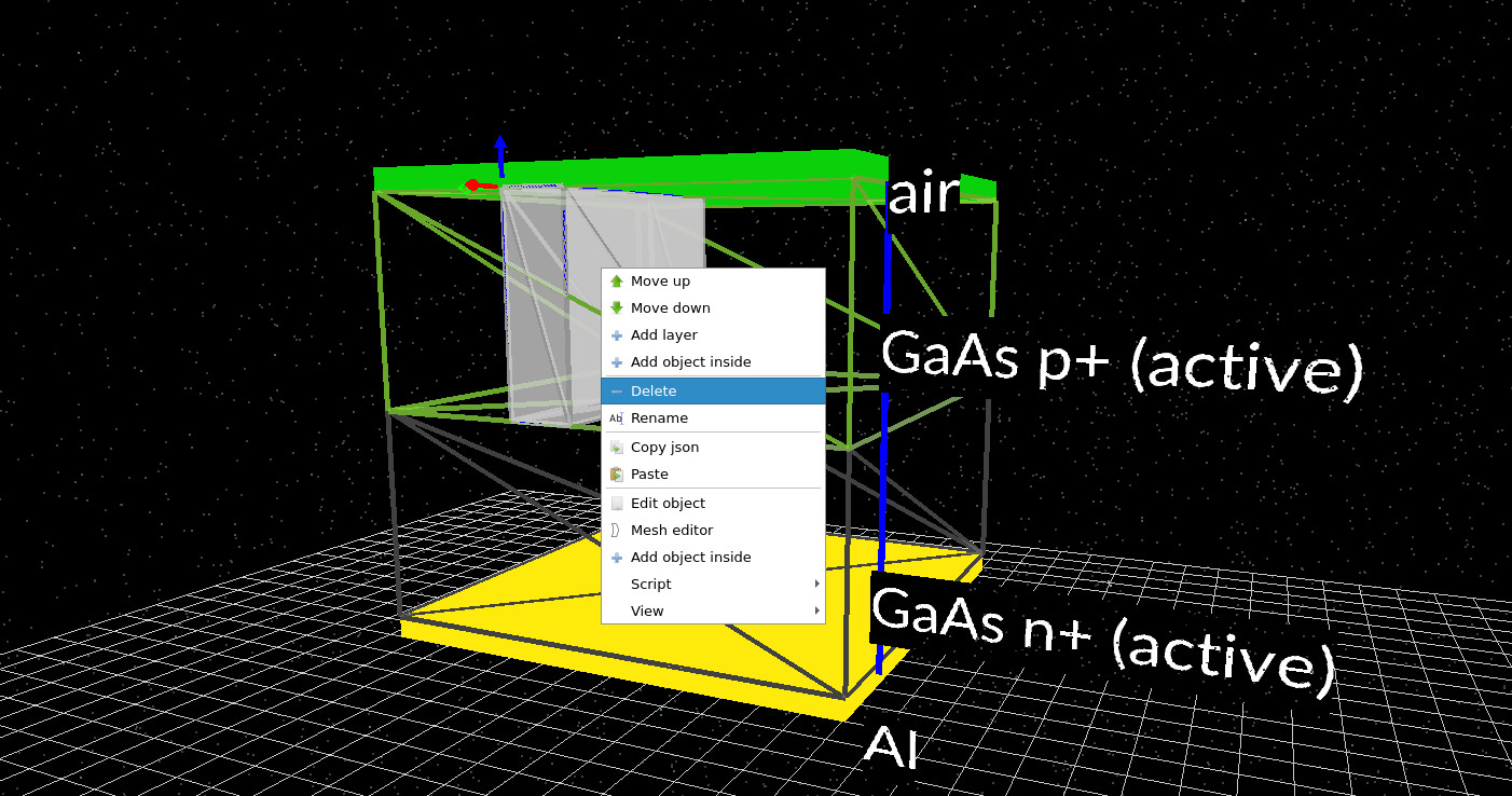
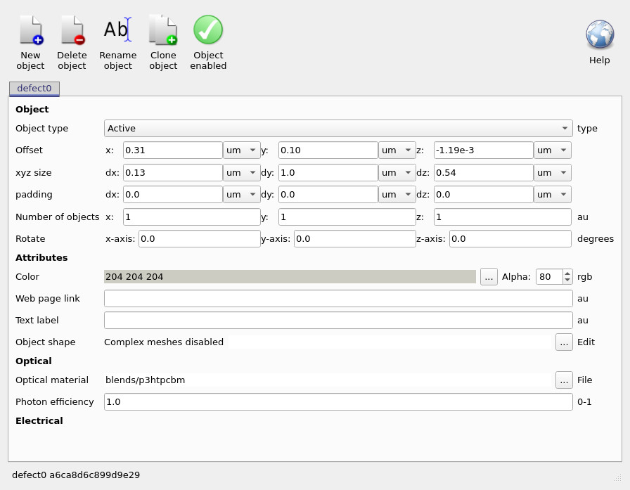
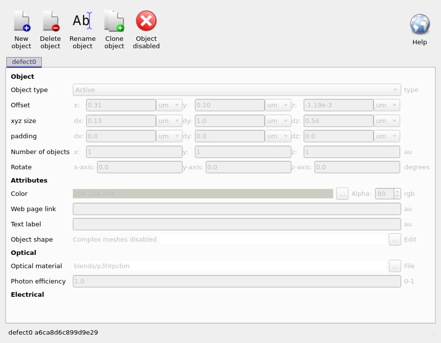
The defect consists of two separate objects. In the 3D device view, right-click one of the defect blocks and select Edit object (not Delete), as shown in ??. This opens the object editor (??), where you can toggle the green Object enabled control. Once disabled, the object is marked with a red cross and its fields are greyed out (??). Repeat this process for the second defect block.
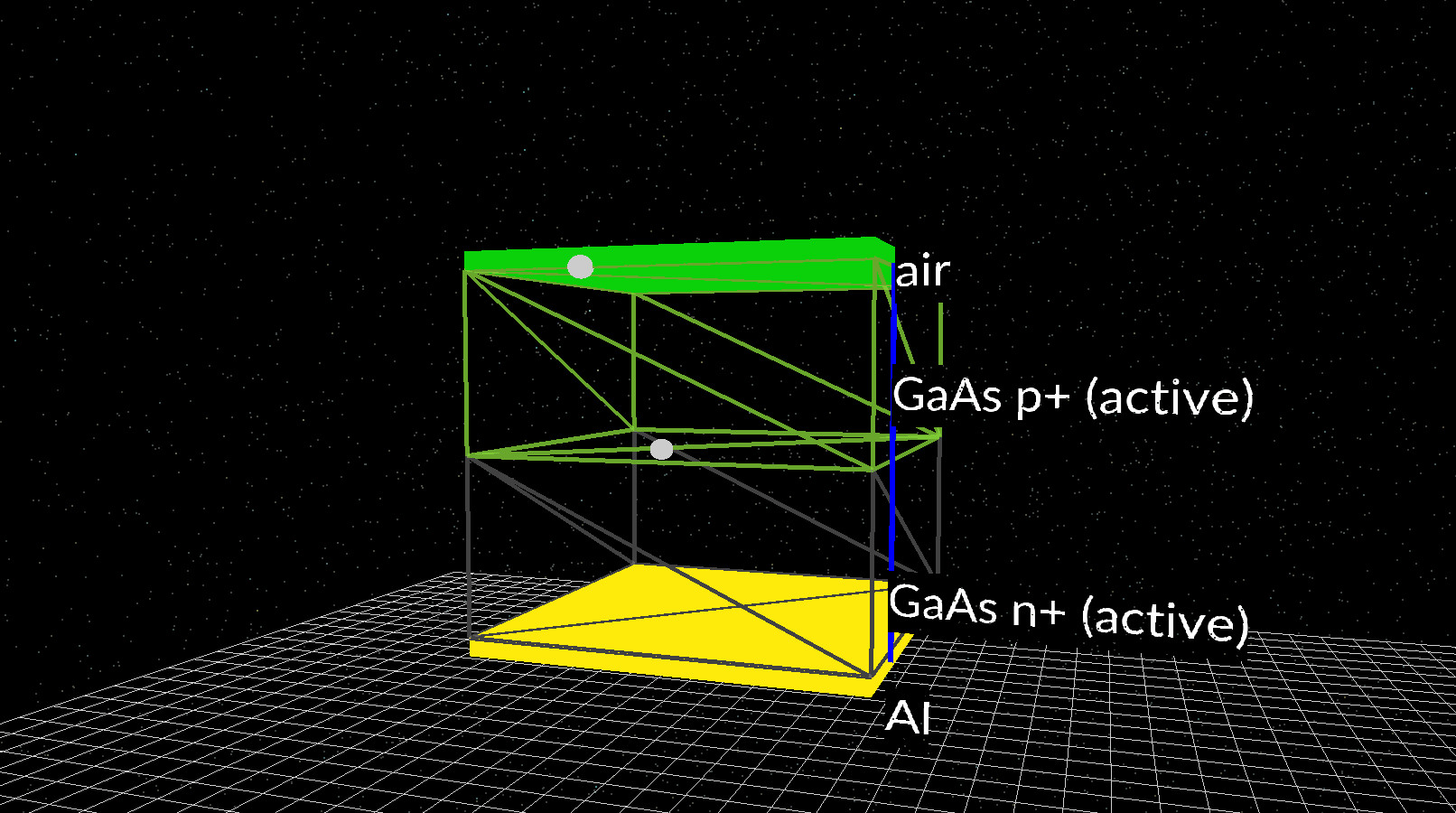
After disabling both defect blocks, the main simulation view should resemble ??. The defect volumes are replaced by small marker spheres, indicating that the objects still exist in the project but no longer participate in the simulation. This restores lateral uniformity while preserving the original geometry, allowing us to change dimensionality in the next step without introducing new physical features.
3. Comparing 3D, 2D and 1D simulations: dimensionality, runtime and results
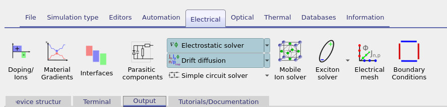
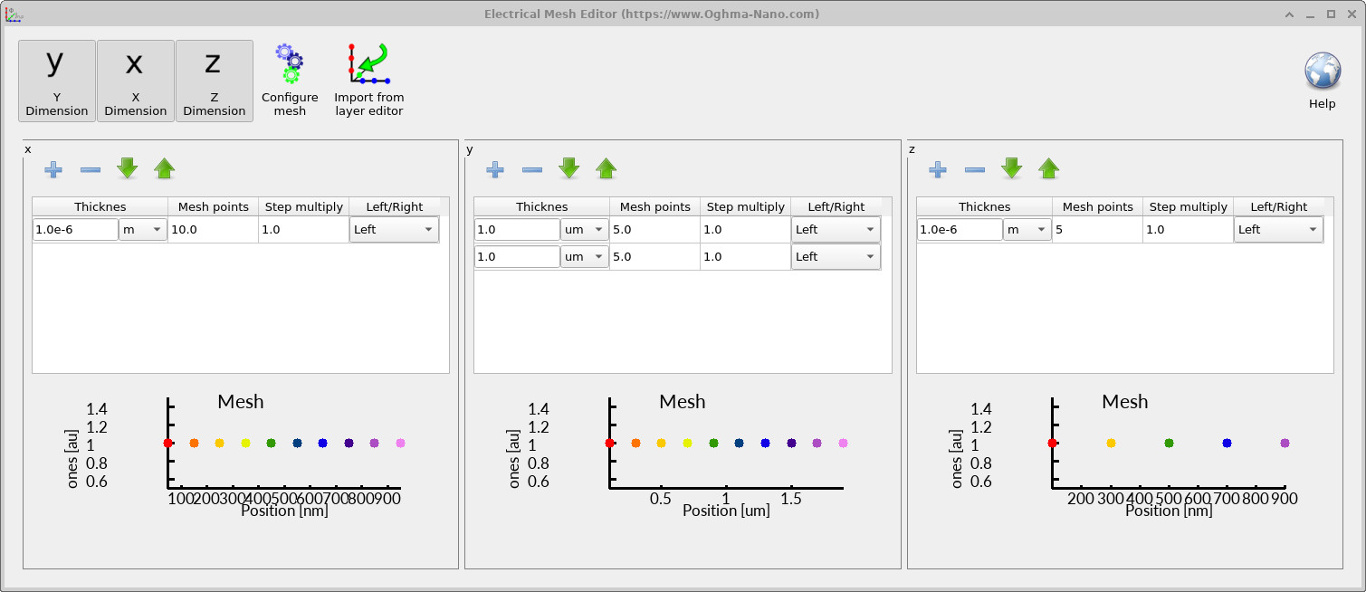
With the defect disabled, the device is now laterally uniform in the x and z directions. This allows us to study the effect of dimensionality alone, without introducing any new physical features. In this section you will run the same GaAs diode as a 3D, 2D, and 1D drift–diffusion problem, compare how long each simulation takes, and verify that the electrical results remain unchanged. Start by opening the Electrical ribbon and clicking Electrical mesh (see ??). First, ensure that x, y, and z are all enabled, so the simulation is fully three-dimensional (??). With the mesh in this state, run the simulation and watch the terminal output as it progresses.
During the run, focus on the timing information printed to the terminal. The right-hand column reports how many milliseconds each simulation step takes (??). On a typical laptop, the 3D case should take on the order of tens to hundreds of milliseconds per step, corresponding to a total runtime of roughly 30 seconds. When the simulation finishes, note the final current value reported at the end of the run (for example, the line corresponding to top = 1.00 V).
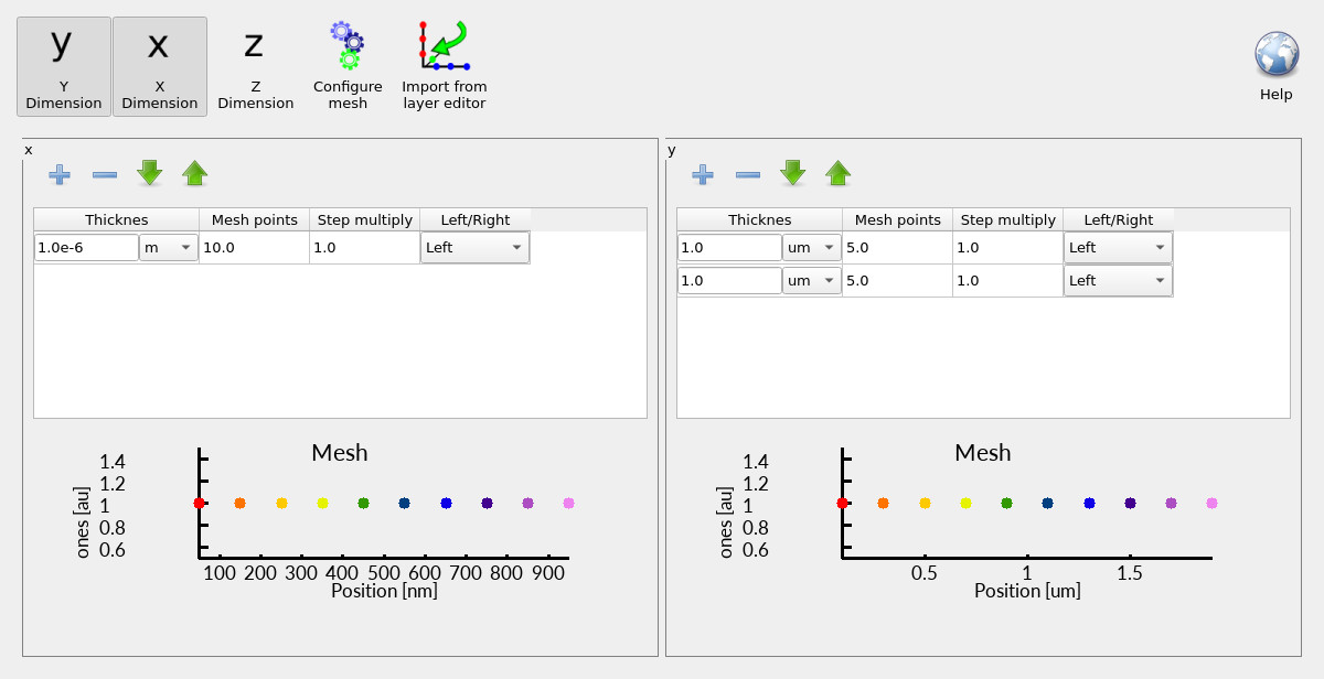
Next, return to the Electrical mesh editor and disable the z direction. The mesh should now represent a 2D (y–x) simulation (??). Run the simulation again and compare the terminal output (??). You should see a dramatic reduction in runtime, with per-step timings dropping to just a few milliseconds. Importantly, the final current value reported at the end of the run should be numerically identical to the 3D case.
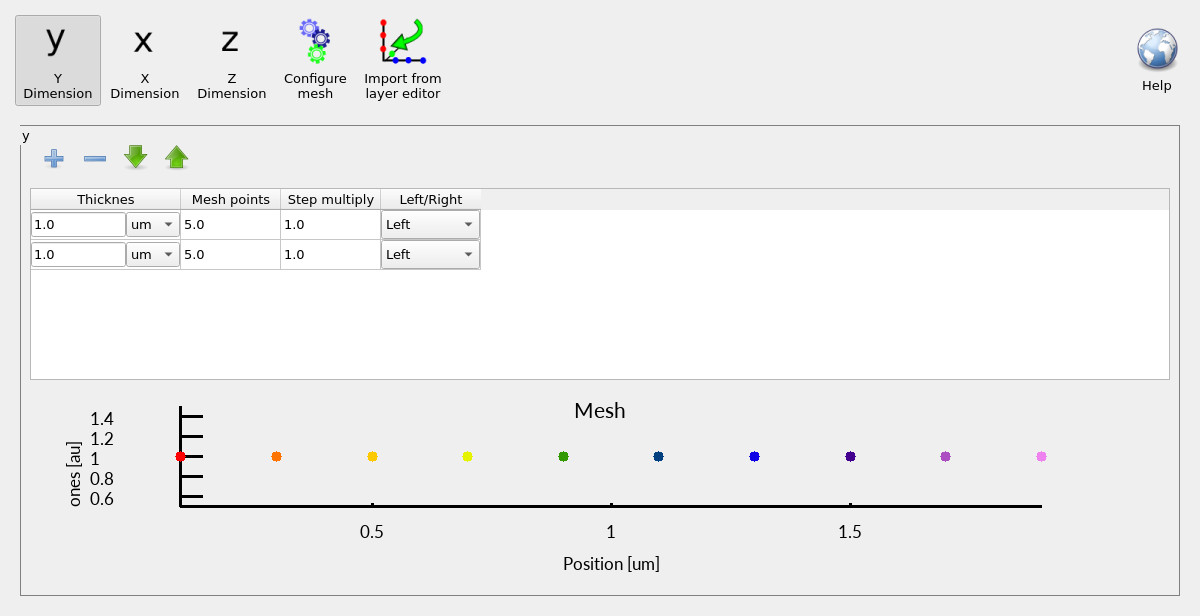
Finally, disable the x direction as well, leaving only the transport direction y. This reduces the problem to a purely 1D drift–diffusion simulation (??). Run the solver one last time and inspect the terminal output (??). In this case the per-step timing is effectively zero, yet the final current at top = 1.00 V is the same as in the 2D and 3D runs.
This comparison illustrates a central principle of device modelling. As dimensionality is reduced, the simulation becomes dramatically faster because the number of unknowns shrinks rapidly (often roughly scaling with the cube of the mesh density). However, because the device is now laterally uniform, reducing dimensionality does not change the physical result. You are solving the same equations for the same structure, just expressed in a more efficient coordinate representation. The key takeaway is that higher dimensionality does not automatically produce different or better physics. It only adds value when the device itself contains genuine lateral variation. Once that variation is removed, 3D, 2D and 1D simulations collapse to the same electrical solution— differing only in computational cost.
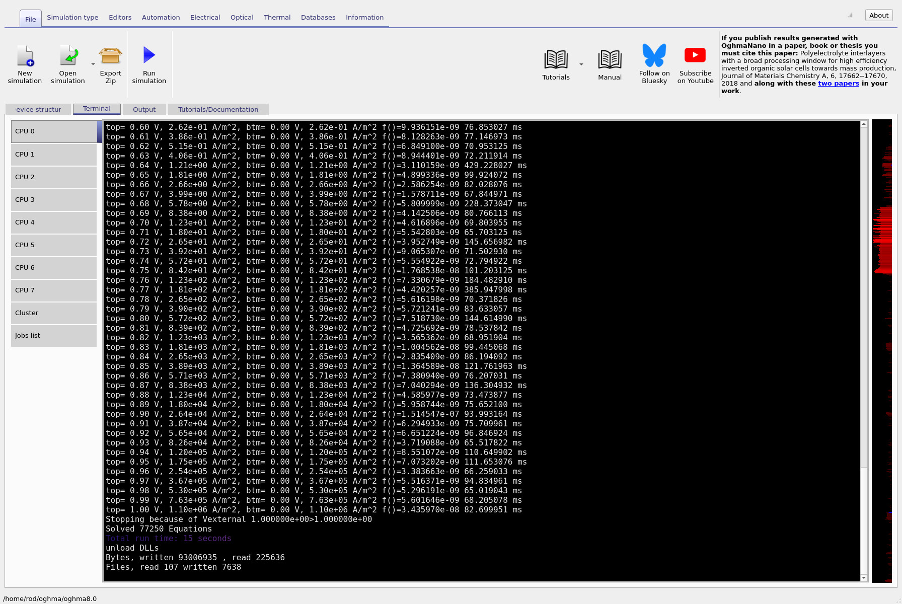

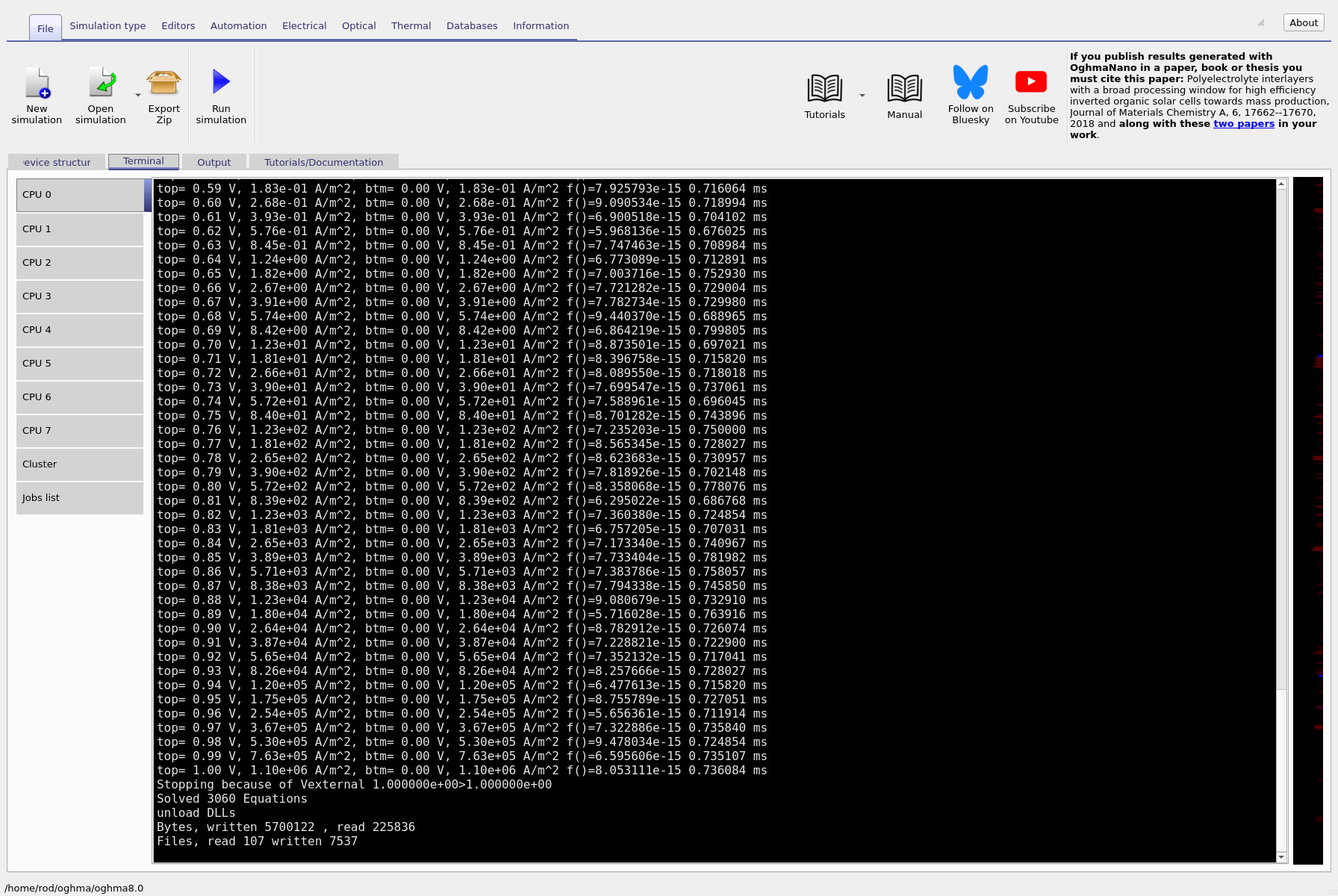
Step 5: Notice the numerical results are identical
Now look closely at the outputs. Pick a single voltage line (for example the entry at top = 1.00 V) and compare the computed currents between the 3D, 2D and 1D runs. You should find the values are the same (to numerical precision). This is the key lesson: once we remove the asymmetry, the device is effectively 1D, so 2D and 3D do not buy you new physics — they only buy you runtime.
That’s it for Part B. In Part C we will look at numerical stability issues that can arise in 2D and 3D simulations, and we will start turning this diode into a solar-cell-like problem by introducing light and observing how illumination changes the device response.
👉 Next step: Continue to Part C, or return to the silicon & semiconductor device overview.