GaAs Tutorial (Part C): Numerical stability & turning the diode into a photodetector
1. Introduction
In this section you will learn why numerical stability becomes a central issue in 2D and 3D drift–diffusion simulations, and why artefacts often appear precisely in the low-current regime. This is not a bug in the software, but a fundamental consequence of solving strongly coupled semiconductor transport equations over extremely large dynamic ranges. Understanding this behaviour is essential when interpreting JV curves, current-density maps, and snapshots from realistic multidimensional device models.
2. Why numerical stability matters more in 2D and 3D
Semiconductor drift–diffusion simulations routinely span very large dynamic ranges. Carrier densities can differ by 10–20+ orders of magnitude between majority and minority regions (for example, heavily doped n-type material versus minority holes). When these scales enter a coupled nonlinear system (Poisson plus electron and hole continuity equations), the resulting Jacobian can become ill-conditioned. In practical terms, this means that small numerical round-off errors can be amplified into visible artefacts, particularly when the true physical current is close to zero.
Most drift–diffusion solvers use double-precision floating point arithmetic. A double has roughly 53 bits of mantissa, corresponding to about 15–16 decimal digits of precision. While this is sufficient for the vast majority of problems, it is not infinite. When equations contain quantities that differ by many orders of magnitude, cancellation, scaling, and matrix conditioning — not raw CPU speed — become the dominant numerical limitations. In 1D, these issues are often less severe because there are fewer degrees of freedom and fewer coupling pathways. In 2D and 3D, additional spatial directions introduce larger matrices and stronger coupling, so numerical sensitivity tends to appear sooner, especially in low-current regimes. In the remainder of this section, you will learn how these numerical effects arise in practice, how they manifest in multidimensional simulations, and how to interpret them correctly when analysing 2D and 3D results.
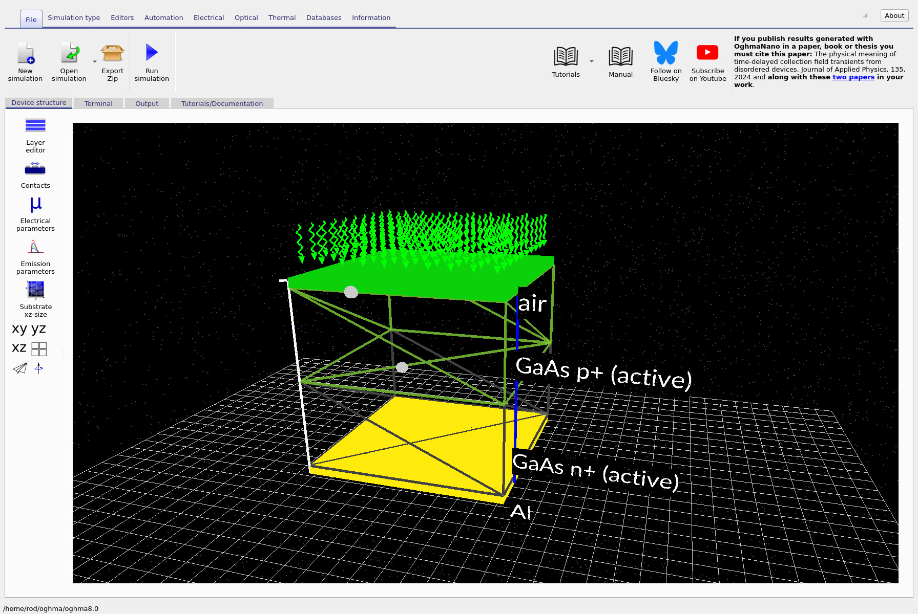
3. Enabling illumination: turning the diode into a photodiode
Up to this point, the GaAs device has been simulated as a dark diode. In this section we enable illumination and observe how the device responds when carriers are generated optically. This allows us to connect the numerical stability discussion from the previous section to a physically meaningful light JV curve, and to see where low-current artefacts tend to appear in practice.
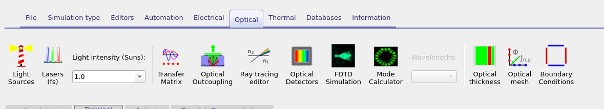
To enable illumination, go to the Optical ribbon (??) and set the Light intensity (Suns) to 1.0. Once enabled, the main device view will show green arrows above the stack, indicating incident photons (??).
🧭 For this section we deliberately use a 2D simulation: open the Electrical mesh editor and ensure that x and y are enabled, while z is disabled. This keeps the runtime short while still exposing the numerical behaviour we want to study.
Run the simulation and open jv_contact0.csv (the top contact).
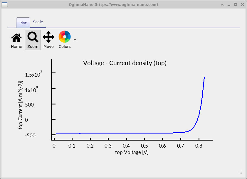
The resulting curve should resemble a physically reasonable illuminated JV characteristic,
but if you zoom in on the low-current region you will often notice small irregularities or
“lumps”
(??).
At this stage two effects are superimposed, and they reinforce one another. First, when the true physical current is close to zero, the numerical sensitivity discussed earlier becomes visible in the extracted JV curve. Second, the absolute photocurrent is relatively small because the structure is still configured as a diode rather than an optimised solar cell. This low photocurrent pushes the operating point deeper into the near-zero-current regime, thereby exacerbating the visibility of numerical artefacts.
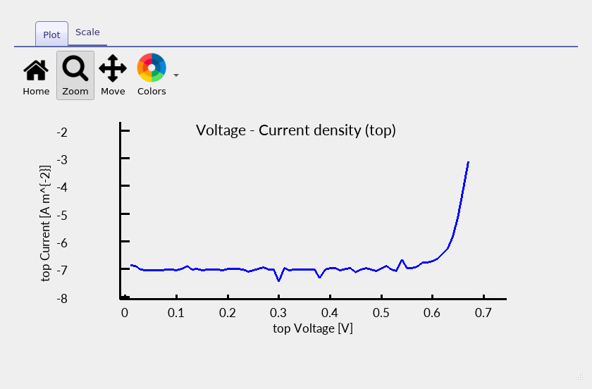
jv_contact0.csv). Low-current lumpiness reflects numerical sensitivity when the true current is close to zero.
4. Diagnosing numerical noise using spatial current-density snapshots
To understand the origin of the small irregularities observed in the light JV curve, it is useful
to inspect what the solver is doing internally.
This can be done using the snapshots/ output, which stores spatially resolved quantities
as a function of simulation step (typically applied bias).
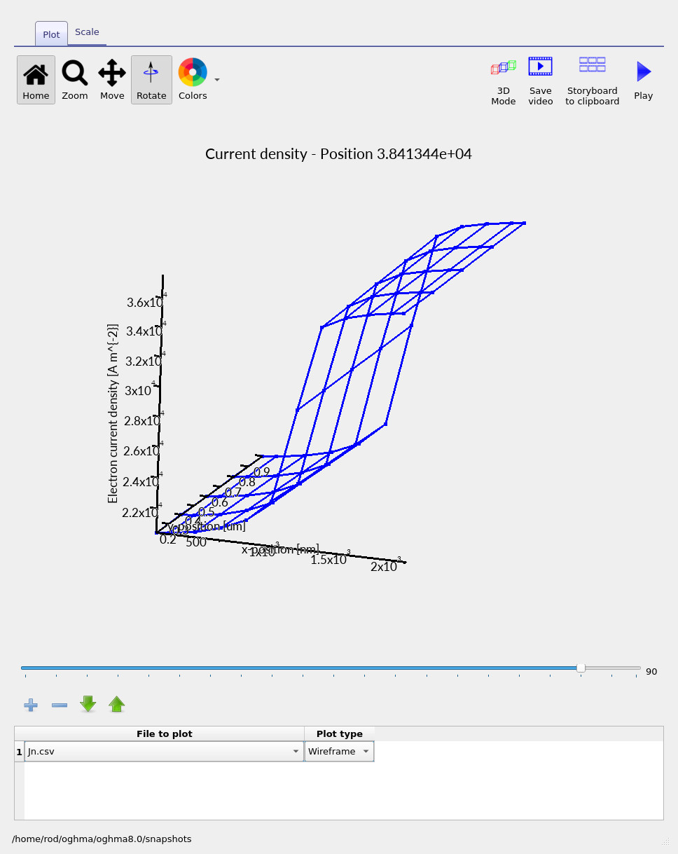
In this section we focus on Jn.csv, the vertical electron current density.
Open the snapshots/ directory and plot Jn.csv.
You should obtain plots similar to
?? and
??,
corresponding to low and higher applied bias, respectively.
At low bias (towards the left of the slider), the absolute magnitude of the current is extremely small.
In this regime the current-density plot can appear spatially irregular:
you are effectively seeing how numerically difficult it is to compute a quantity that is
physically close to zero.
As the bias increases and the current becomes appreciably non-zero, the spatial distribution
of Jn.csv becomes smoother and more physically intuitive.
These small spatial irregularities at very low current feed directly into the extracted JV curve,
which is why the low-current region of the JV can appear slightly “lumpy”.
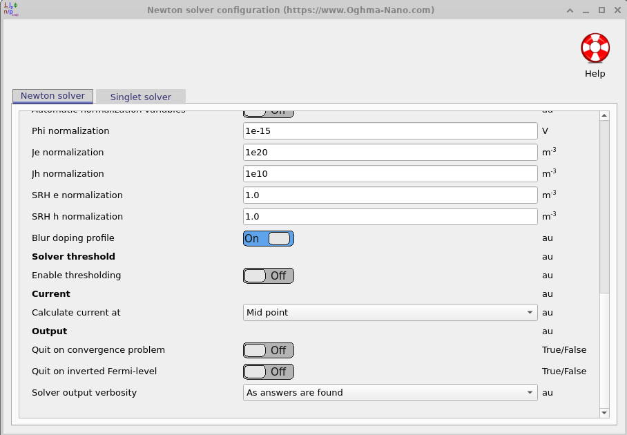
One practical way to reduce the visibility of these artefacts is to change where the current is evaluated. Currents evaluated very close to contacts tend to be more sensitive to numerical noise than currents evaluated in the interior of the device. In this tutorial the current is already evaluated at the mid point of the device, a setting that can be found under the Electrical ribbon in the Drift diffusion → Solver configuration menu. Evaluating the current at the mid point reduces sensitivity to boundary effects and typically produces a cleaner JV curve in low-current regimes.
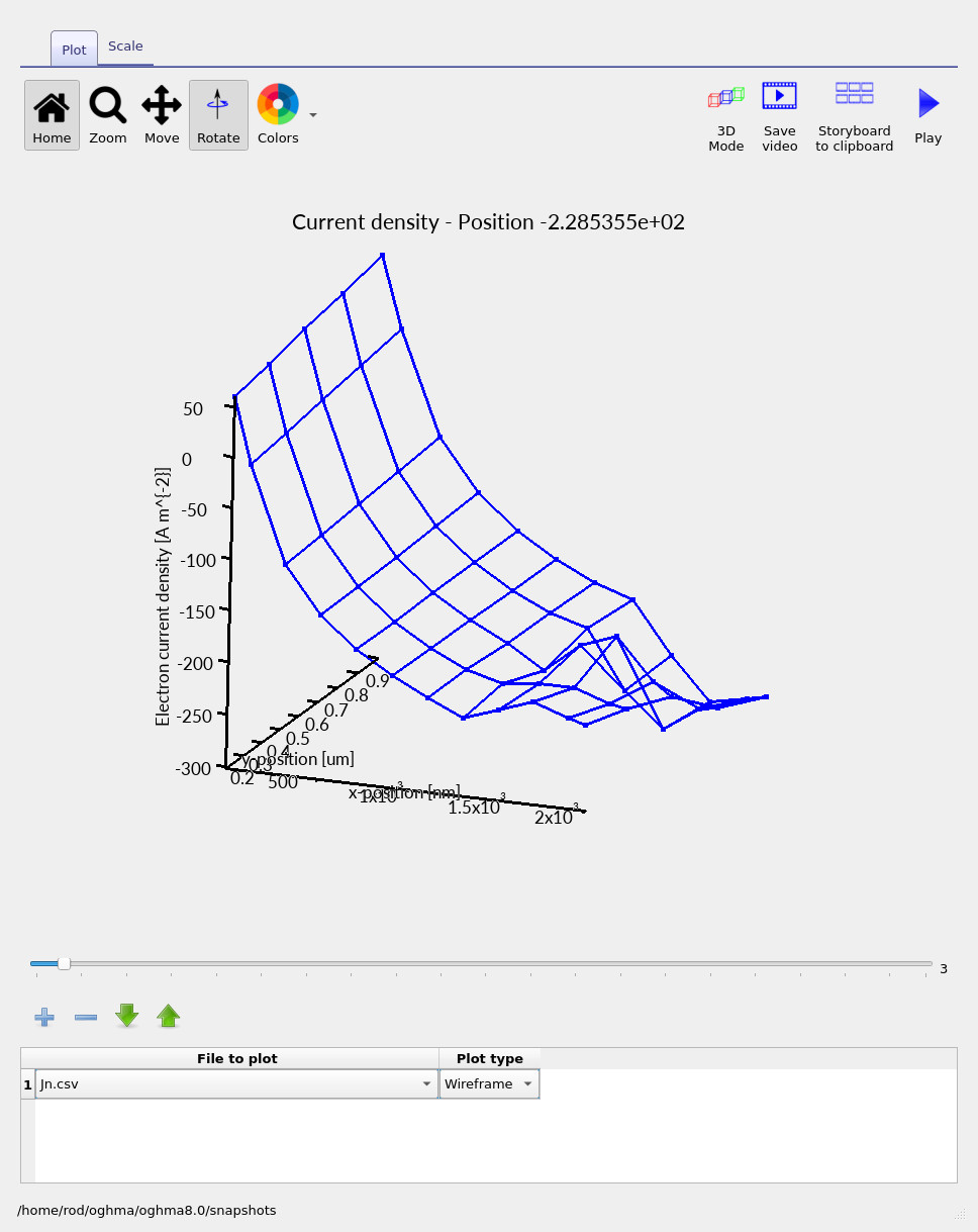
Jn.csv at low bias in 2D. The true current is very small, so numerical sensitivity becomes visible.
Jn.csv at higher bias. Once the current is appreciably non-zero, the spatial profile becomes smoother and more physical.
5. Fixing low photocurrent: don’t shine through thick metal
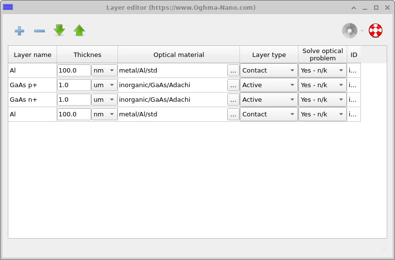
You may have noticed that the photocurrent obtained so far is lower than one would normally expect for a GaAs device. In this example, that behaviour is largely intentional. The structure was originally designed as a diode, not as an optimised photodiode or solar cell: the top aluminium contact is sufficiently thick that it strongly reflects and absorbs incident light. In other words, the simulation is effectively attempting to “shine through metal”.
To correct this, open the Layer editor (??) and reduce the thickness of the aluminium (Al) top contact from 100 nm to 10 nm. Re-run the simulation and re-open the illuminated JV curve.
You should now observe a substantially larger photocurrent and a much smoother low-current region. This improvement does not come from changing the numerical method, but from increasing the true physical signal. By moving the device away from the near-zero-current regime, the numerical floor is effectively pushed out of view and the previously visible artefacts disappear.
6. Summary and key takeaways
Across this three-part tutorial you have explored how dimensionality, numerical stability, and physical configuration interact in drift–diffusion simulations:
-
In Part A, you ran a fully 3D GaAs diode containing an intentional vertical defect,
visualised current crowding, and inspected internal variables using
snapshots/. - In Part B, you removed the defect and demonstrated that once the structure becomes laterally uniform, 3D, 2D, and 1D simulations produce the same electrical result — while runtime changes by orders of magnitude.
- In Part C, you enabled illumination to create a photodevice, used spatial current-density plots to diagnose numerical sensitivity, and showed how low photocurrent amplifies visible artefacts.
Core insight: numerical artefacts are most visible when the true physical current is close to zero. Low-current regimes — whether caused by bias conditions, recombination, or optical blocking — are inherently the hardest cases for any drift–diffusion solver. Once the current becomes appreciably non-zero, the same numerical method typically appears much smoother.
Where to go next: explore how numerical stability evolves as you increase dynamic range. Useful directions include sweeping SRH or Auger recombination parameters, varying doping or mobility contrasts, increasing illumination intensity, or introducing more realistic contact selectivity. Each of these pushes the solver in different ways and helps build intuition for when higher-dimensional modelling is both necessary and numerically robust.