Large-area organic solar cell simulation (PM6:Y6): From 3D contact networks to illuminated devices
1. Introduction
In this tutorial we continue the series on large-area device simulation, focusing on devices that have moved beyond small laboratory cells and into application-scale geometries. It sits between two existing workflows in the manual: designing large-area contacts (without active devices), and complex 3D perovskite modules. This example bridges those two, introducing diodes and light absorption into a previously designed contact structure, but stopping short of a fully interconnected module.
Here we simulate a single large-area organic solar cell based on a PM6:Y6-type architecture with printed, hexagonal metal contacts. The aim is to understand how a device that performs well at small area behaves when scaled up, where lateral current flow, voltage drop, and contact resistance begin to dominate. Although this tutorial uses OPV materials, the workflow is general: by swapping the optical n/k data and adjusting component values, the same model can represent your research device.
To apply this workflow to your own device, you simply provide two sets of inputs: layer resistivities (typically taken from the literature or simple test structures), and a small number of diode parameters such as the ideality factor, photocurrent, and saturation current. Once these are set, the model allows you to virtually upscale a laboratory-scale device and identify which loss mechanisms will limit its efficiency when moved to large-area, real-world geometries.
Here we do not use the full 3D drift-diffusion solver, although OghmaNano does provide one. For large-area devices, fully resolved 3D drift-diffusion quickly becomes computationally impractical and is often unnecessary when the dominant limitations arise from lateral transport and contact resistance rather than carrier motion through every layer. Instead, OghmaNano constructs a geometry-aware 3D circuit model, where lateral transport and contacts are represented by resistive elements and the photovoltaic behaviour is captured using embedded diodes.
While the electrical problem is solved using a circuit formulation, the optics are treated rigorously. Photogeneration is computed using a transfer-matrix optical solver evaluated in one-dimensional slices across the three-dimensional geometry, retaining thin-film interference and absorption effects while the circuit solver handles large-area current collection.
2. Create the simulation
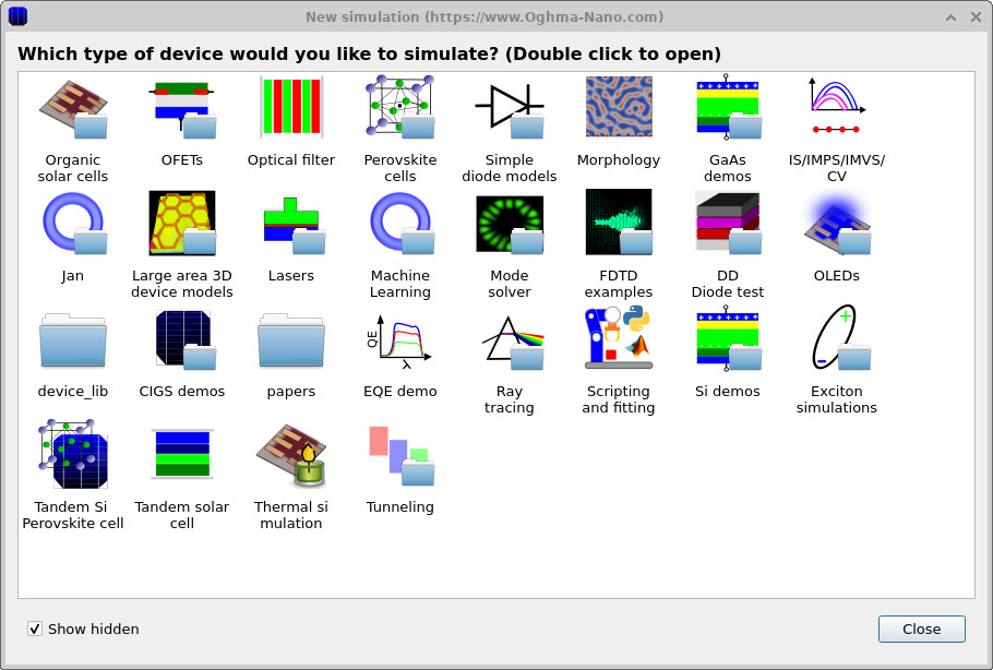
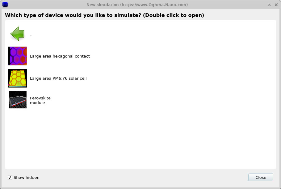
In the main window, click New simulation. You will see a list of simulation categories (see ??). Then double-click Large area PM6:Y6 solar cell (see ??).
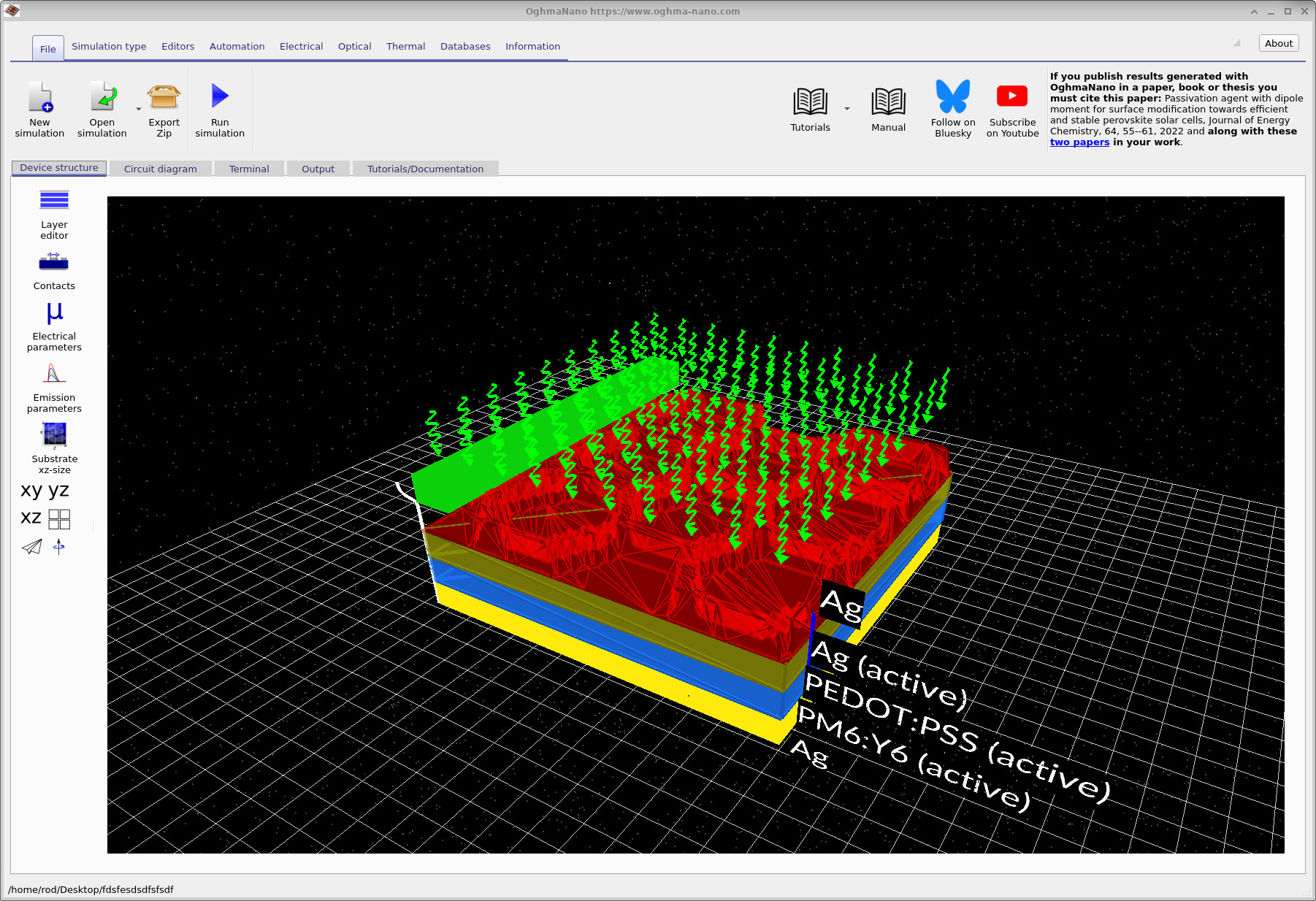
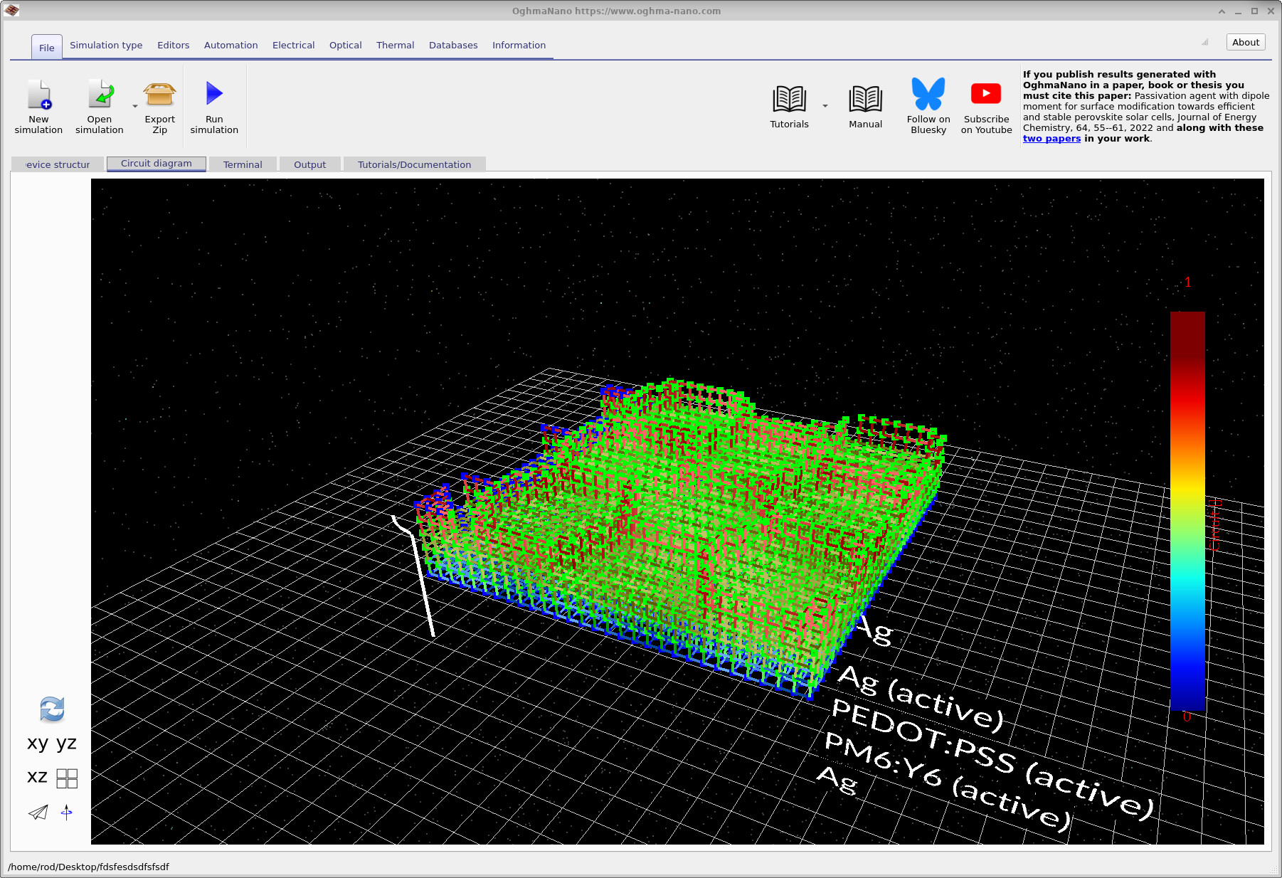
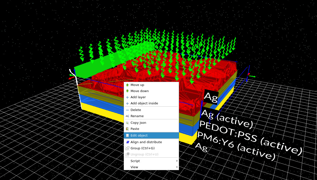
After creating the simulation, the main window opens and displays the device geometry in three dimensions (see ??). The top contact is a hexagonal (honeycomb) metal mesh labelled Ag. This silver layer acts as a highly conductive current collection grid. Because it is implemented as a mesh, most of the surface remains open, allowing light to pass through the contact. Beneath the silver mesh sits PEDOT:PSS, which serves as a lateral current-spreading layer. As in the large-area contact tutorial, charge is first collected laterally in the polymer layer and then transferred into the low-resistance silver grid for efficient extraction.
The photoactive layer is PM6:Y6. Electrically, this layer is represented by a diode element with optical generation enabled, while additional resistive components ensure the solver accounts for its finite conductivity. At the bottom of the stack is a continuous Ag contact that spans the full device area and completes the electrical connection.
The green bar visible in the main window may appear to be floating, but it is simply a visual indicator of the extraction boundary condition. It marks the region where the solver applies the electrical contact used to extract current from the circuit network.
3. Inspect the epitaxial layer stack and contacts
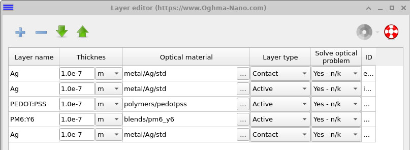
This simulation (and the earlier large-area contact example) is defined using a layered epitaxial structure. The device is constructed as a stack of thin-film layers using the layer editor, which ensures that each layer sits cleanly on top of the next, with no gaps and consistent handling of thickness. This approach is well suited to planar large-area devices, where the vertical stack is fixed and lateral behaviour is introduced through the circuit model. It differs from later module-style simulations (see the interconnected module tutorial), where fingers, busbars, and more complex layouts are defined explicitly using full 3D geometry.
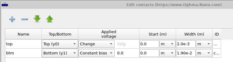
To inspect the structure, open the Layer editor to view the layer stack (see ??), and then open the Contacts panel in the device structure editor (see ??). Geometrically, the configuration is simple but important: the bottom contact spans the full device area, while the top contact is much smaller and defines the region where current is extracted, consistent with the green extraction marker shown in the 3D view. Understanding this contact geometry is essential, as it sets the lateral current paths that dominate large-area device behaviour.
4. Inspecting the mesh
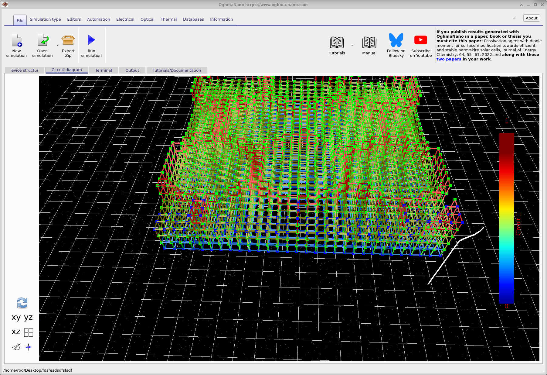
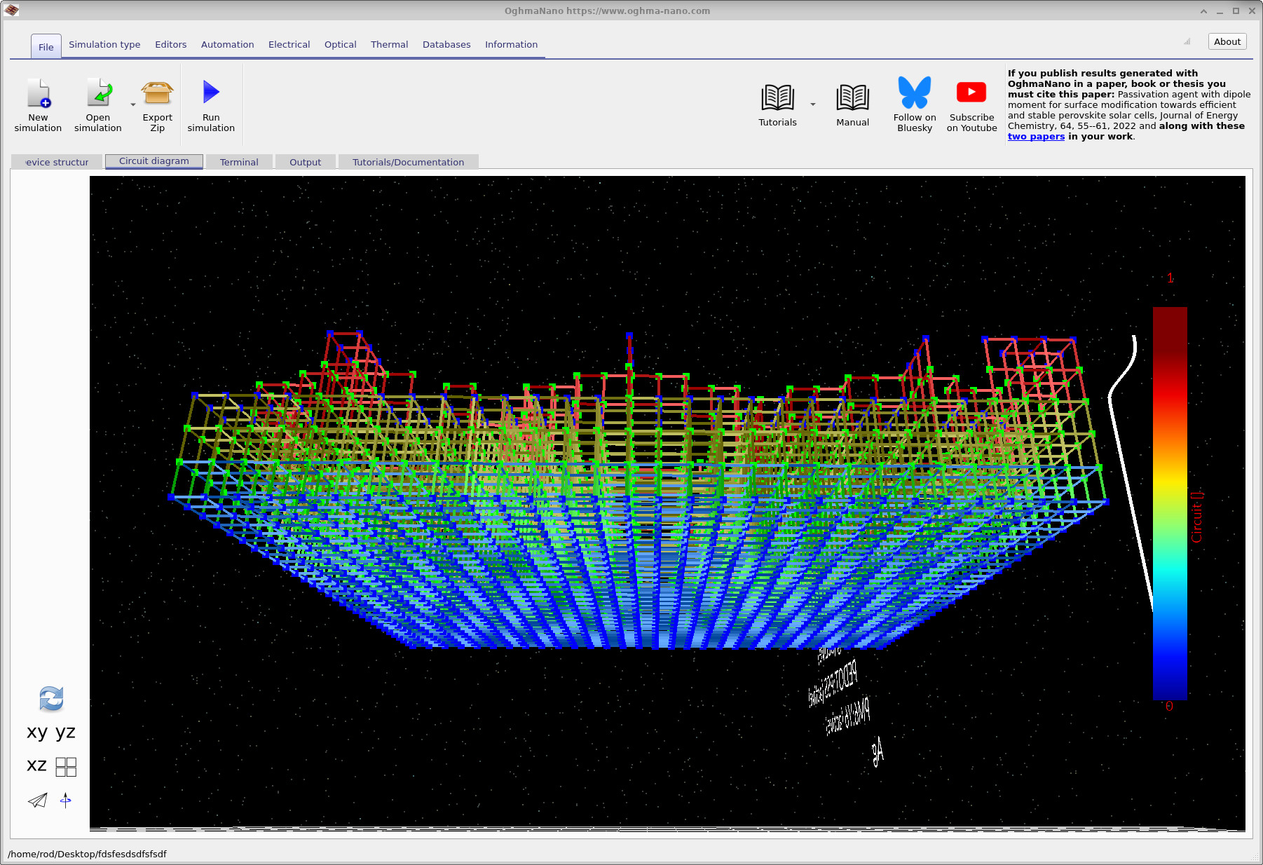
Switch to the Circuit diagram tab and click the refresh icon at the bottom left (the recycle-style button). This action builds the circuit representation of the device directly from the defined geometry and layer stack. The resulting circuit mesh is shown in ??. Each link in the mesh corresponds to a circuit element, such as a resistor or diode, with the colour indicating the layer or material region from which it originates.
By rotating the view, you can clearly identify the top and bottom contact regions. In ?? and ??, the blue dots indicate the nodes where current is extracted from the circuit mesh. These nodes define the contact boundary conditions and represent the locations at which the circuit solver collects current from the device.
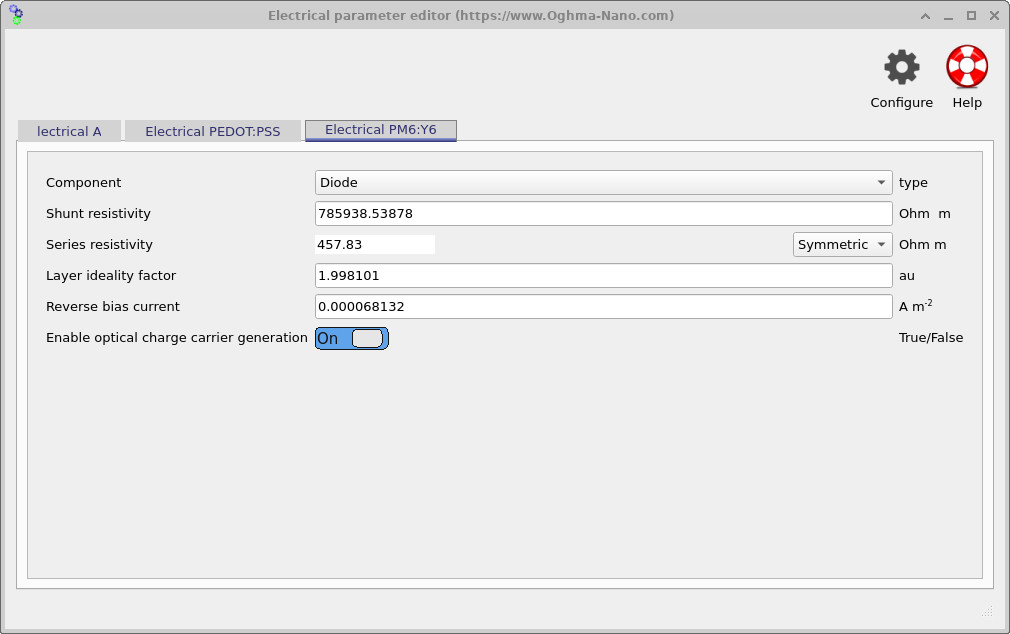
5. Electrical parameters and optical generation
Open Electrical parameters from the device structure panel. This editor controls the resistor and diode properties used by the large-area circuit model. Example settings are shown in ?? and ??. For the PM6:Y6 layer you will see parameters specific to a diode element, including the ideality factor n and the reverse-bias (saturation) current I0. If you replace these values with values from your own experimental curves you will see how your device will up-scale. You can also enable optical charge-carrier generation. When optical generation is enabled, the transfer-matrix optical solver provides a photogeneration term that enters the electrical model as a photocurrent Iph in the illuminated diode equation:
I(V) = I0 [ exp( qV / (n k T) ) − 1 ] − Iph
In this tutorial, the toggle effectively controls the Iph term. With optical generation disabled, the circuit behaves as a dark diode network. With it enabled, illumination injects current into the circuit through the diode element, with Iph determined by the absorbed photon flux from the transfer-matrix optics.
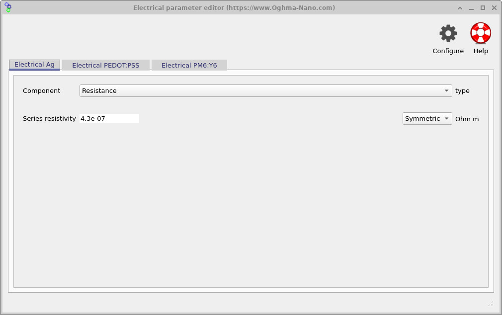
💡 Implementation detail: the active layer may be discretised into multiple resistive elements through its thickness to capture bulk transport and series resistance. However, the circuit model always contains a single diode layer, typically placed at the bottom of the active region. This reflects the fact that the diode represents the overall JV response and photogeneration of the device, while the resistive elements account for voltage drop and current spreading within the material.
6. Running the simulation
To start the simulation, click Run simulation (the blue triangle in the main toolbar), or press F9. The solver will immediately begin executing, and the output terminal will update in real time (see ??).
The coloured lines that appear early in the output correspond to the optical calculation. At this stage, the transfer-matrix solver is evaluating photogeneration across the device, slice by slice, to build the spatially resolved generation profile. Once this is complete, the solver moves on to the electrical problem and begins solving the circuit network.
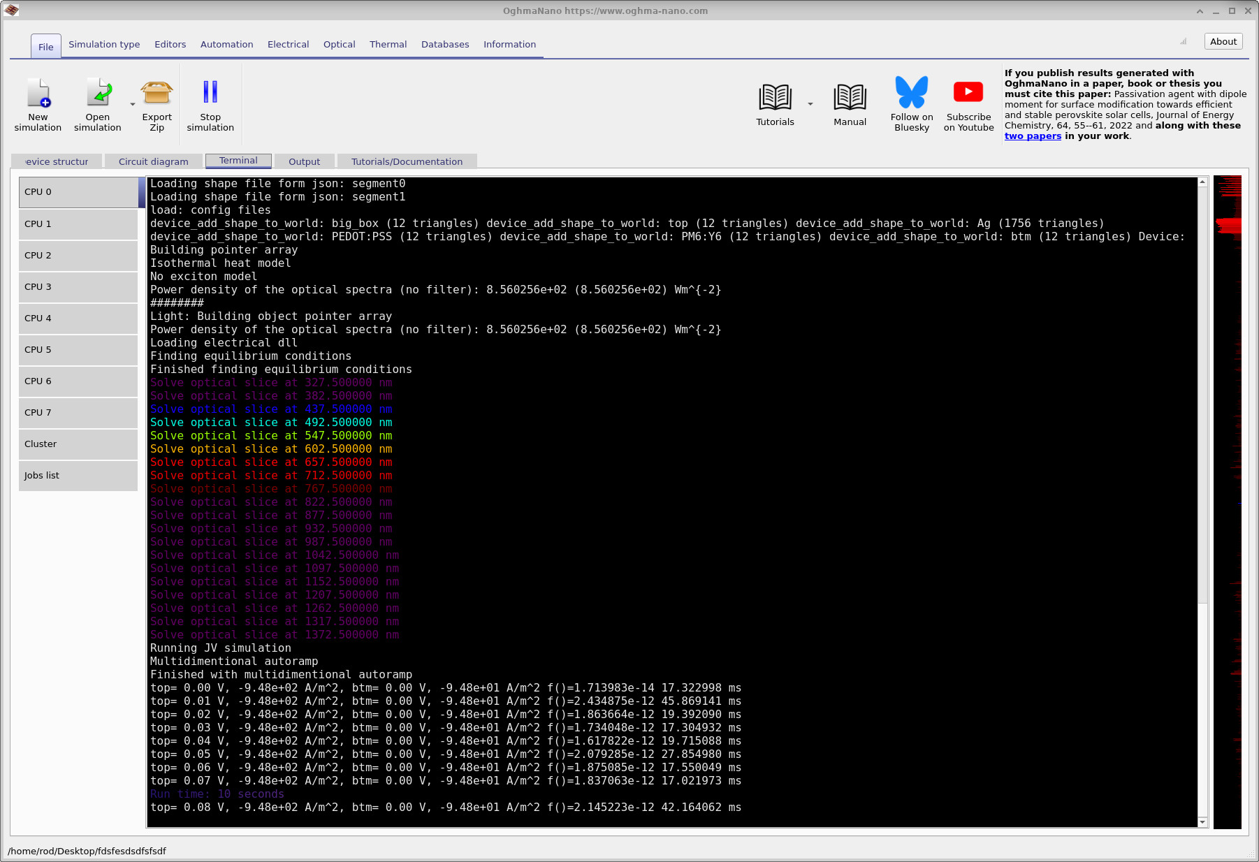
It is worth paying attention to the terminal output as the simulation runs. This information is not diagnostic noise: it provides useful insight into whether the simulation is behaving physically. In the snapshot shown, we can see that approximately −9.48 × 10² A m−2 is flowing out of one contact, while −9.48 × 101 A m−2 is flowing out of the other. At the same time, the reported solver residual F = 1.7 × 10⁻¹⁴ indicates that current continuity has been satisfied to extremely high precision, with the first JV point solved in around 17 ms.
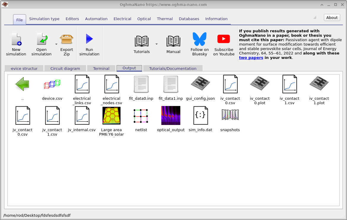
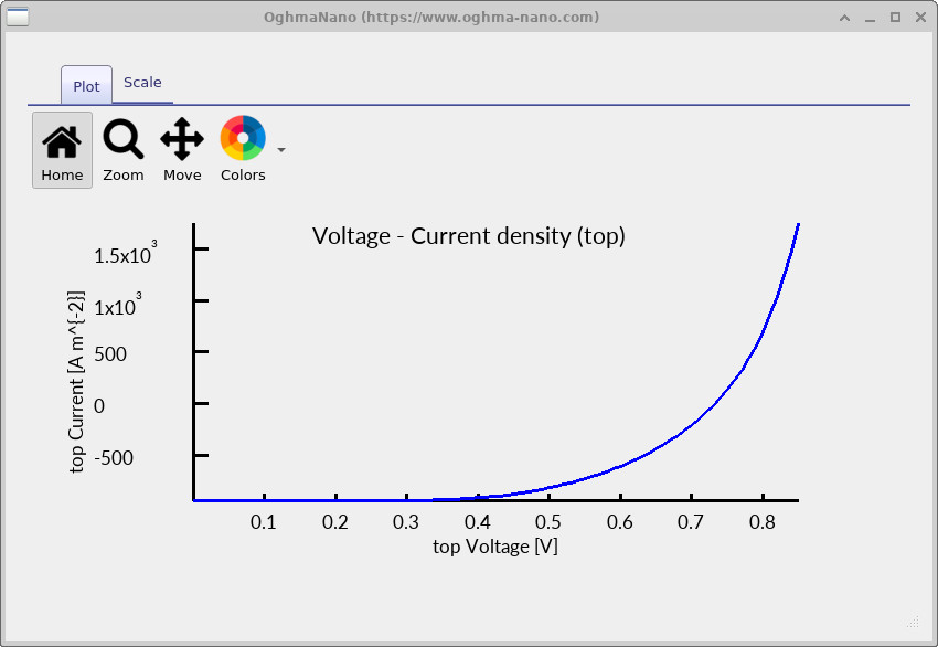
The difference in current density between the two contacts is entirely expected. The bottom contact spans the full device area, while the top contact occupies only a small region. As a result, the same total current is extracted through a much smaller area at the top contact, leading to a significantly higher current density there. Reading the terminal output in this way provides a quick and effective sanity check that the simulation geometry and boundary conditions are physically consistent. If the residual error were to increase to order unity, or if the runtime became unusually long, it would usually indicate a problem such as a broken mesh or a disconnected contact. Once the simulation completes, open the Output tab (see ??). The available outputs are described in more detail in the previous tutorial and explored further in the next tutorial. Here, we focus only on the contact-resolved JV curves.
Each electrical contact has its own JV file, jv_contact0.csv and jv_contact1.csv, which record the current flowing out of that specific contact. Although the current densities differ, the total extracted current is the same once the contact areas are taken into account. Opening jv_contact0.csv produces the JV curve shown below.
7. Editing material parameters
Material properties can be modified directly through the object editor. By right-clicking on any layer in the 3D view and selecting Edit object, the object editor opens (see ?? and ??).
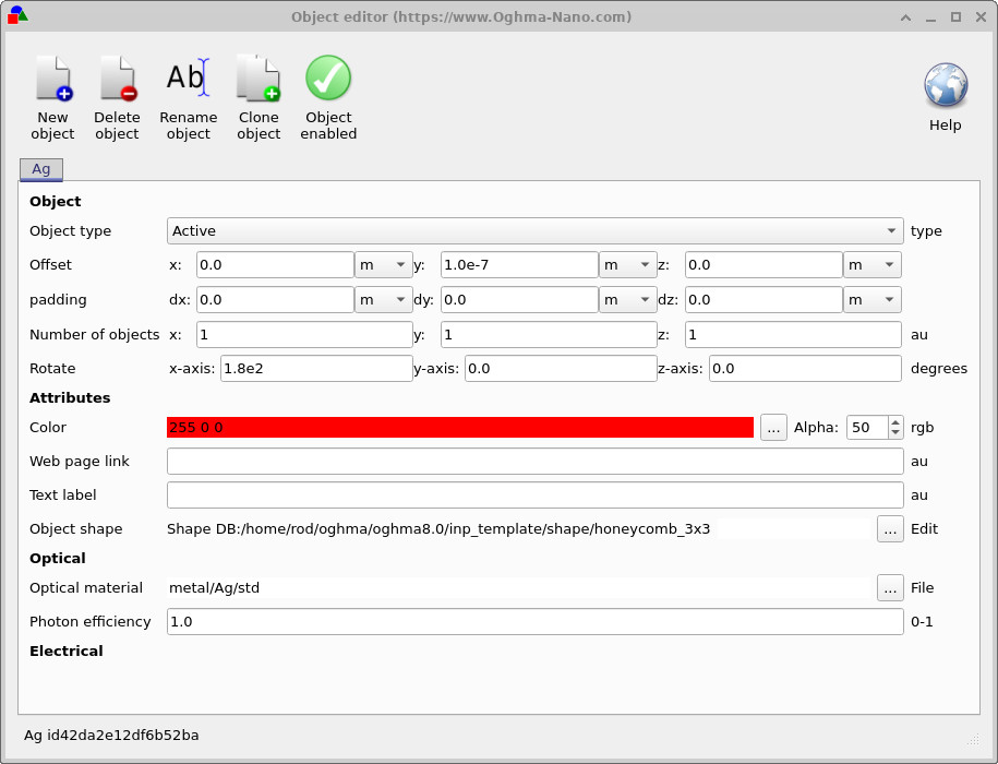
From here, you can change the optical material assigned to the object, modify its geometric shape (for example when using patterned contacts such as honeycomb meshes), or adjust visual attributes such as colour. In this epitaxial-style simulation, the absolute object position is largely defined by the layer stack, so parameters such as translation and rotation usually have little effect. What matters most are the optical material assignment and the object geometry.
💡 Try this: right-click on the PM6:Y6 layer and replace its optical material with a perovskite. Then rerun the simulation and observe how the JV curve changes. If you wish, you can also update the diode parameters — such as the ideality factor, saturation current, and photocurrent — using values reported in the perovskite literature.
📘 Return to the introduction to organic electronics for a broader overview of the topic.