Large-area device simulation – Part A: Setting up and understanding a 3D contact model
Large-area optoelectronic devices – such as flexible solar cells, perovskite modules, OLED panels, and printed electronics – are often limited not by the active semiconductor, but by the electrical contacts. As device area increases, current must travel laterally through transparent conductors before reaching a highly conducting external contact. The resulting resistive losses can dramatically reduce efficiency, fill factor, or brightness uniformity.
A common solution is to combine a conducting polymer or transparent conductor (for local current collection) with a metallic mesh (for long-range current transport). The mesh may be hexagonal, square, finger-based, or entirely custom. Designing such contacts experimentally is expensive: lithography, printing, and process optimisation all carry significant cost. Numerical simulation provides a way to estimate resistance, voltage drop, and current crowding before fabrication.
In this tutorial we focus exclusively on the contact itself. The structure shown here is not a full solar cell or LED; rather, it is a reusable contact model that could sit on top of any device. Later tutorials show how to integrate these contacts with full optoelectronic stacks. Here, our goal is to understand how current flows through the contact and where losses arise.
Step 1: Create a new large-area contact simulation
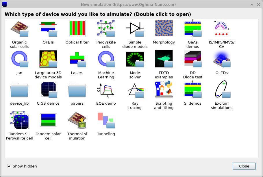
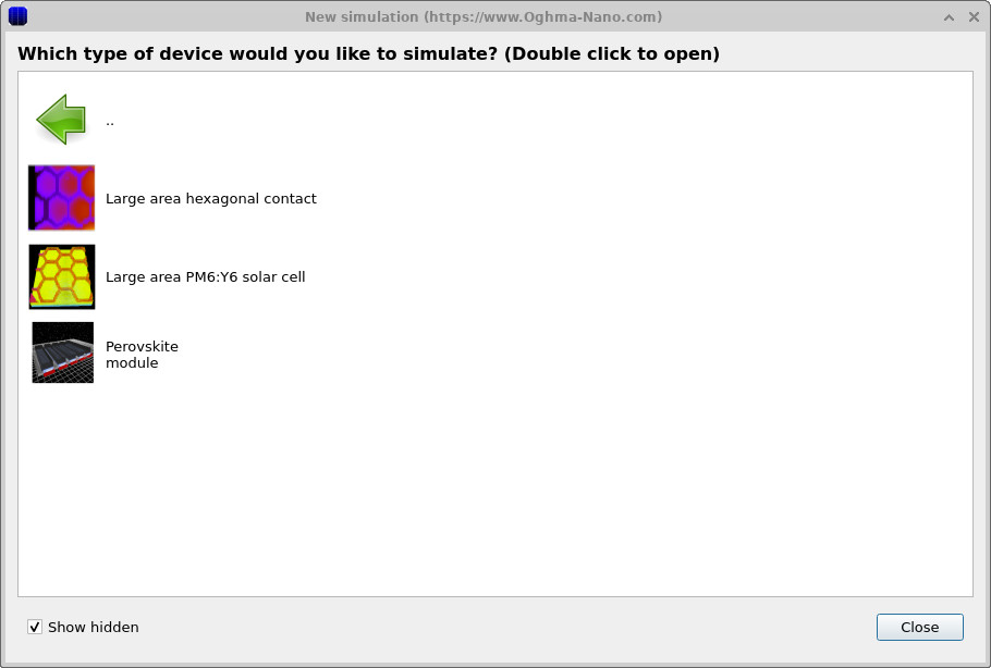
From the main OghmaNano window, click New simulation. In the simulation library, double‑click Large area 3D device models, as shown in ??. This opens a list of predefined large-area structures (??). Double‑click Large area hexagonal contact.
Step 2: Inspecting the contact structure
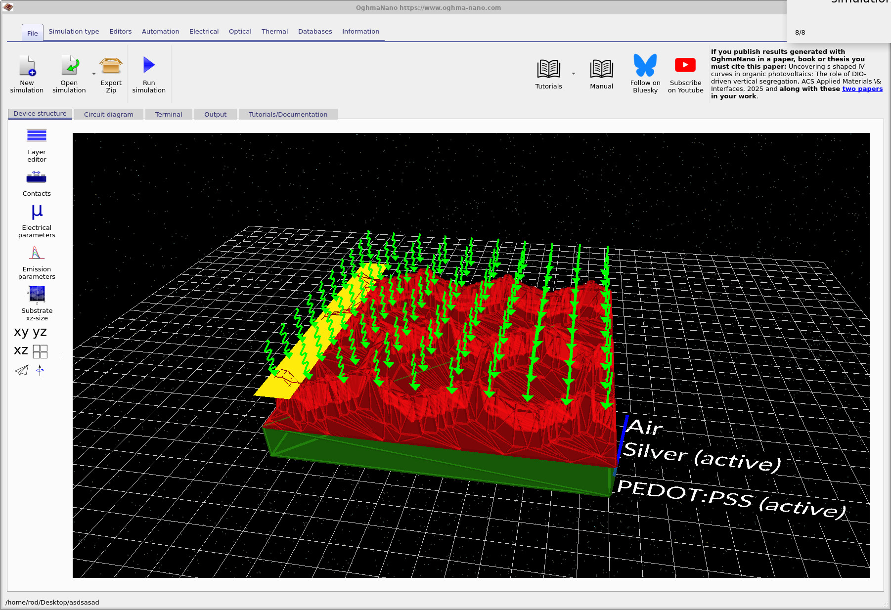
The main simulation window now opens (??). This structure represents a stand‑alone electrical contact. It is not yet attached to a photovoltaic or light‑emitting device; instead, it models how current flows within the contact layers themselves.
You can rotate the view by dragging the star‑field background. The key features are:
- Metallic mesh (red) – a highly conducting network (here hexagonal) that transports current over long distances.
- Conducting polymer (green) – a lower‑conductivity layer (here PEDOT:PSS) that collects current locally and feeds it into the mesh.
- Extraction bar (yellow) – the external electrode where current is ultimately removed from the device.
Although this example uses a hexagonal mesh and PEDOT:PSS, neither is fundamental. You can replace the mesh with arbitrary geometries and the polymer with any conductive layer. The purpose of this tutorial is to understand the electrical consequences of such design choices.
Step 3: Layer and contact definitions
Open the Layer editor to view the defined layers (??). Three layers are present:
- Air – a placeholder layer that hosts the top contact.
- Silver – the metallic mesh layer.
- PEDOT:PSS – the conducting polymer layer beneath the mesh.
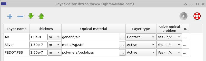
Note that the air layer is marked as a Contact, while the silver and polymer layers are marked as Active. In this context, “active” simply means that OghmaNano solves the electrical equations there. No semiconductor drift–diffusion physics is used in this example.
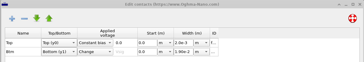
Open the Contacts editor (??). Two contacts are defined: a top contact held at 0 V, and a bottom contact whose voltage will be swept in later simulations. The contact widths define the physical region over which current is injected or extracted.
Step 4: Building the 3D circuit representation
Because this is a large-area metallic and polymeric structure, solving full semiconductor drift–diffusion equations would be unnecessary and inefficient. Instead, OghmaNano treats this model as a 3D resistive network governed by Kirchhoff’s current and voltage laws. Each small volume element becomes a resistor, and the entire structure is solved as a large circuit.
Switch to the Circuit diagram tab and click the recycle icon in the bottom‑left corner. This generates the 3D circuit representation shown below.
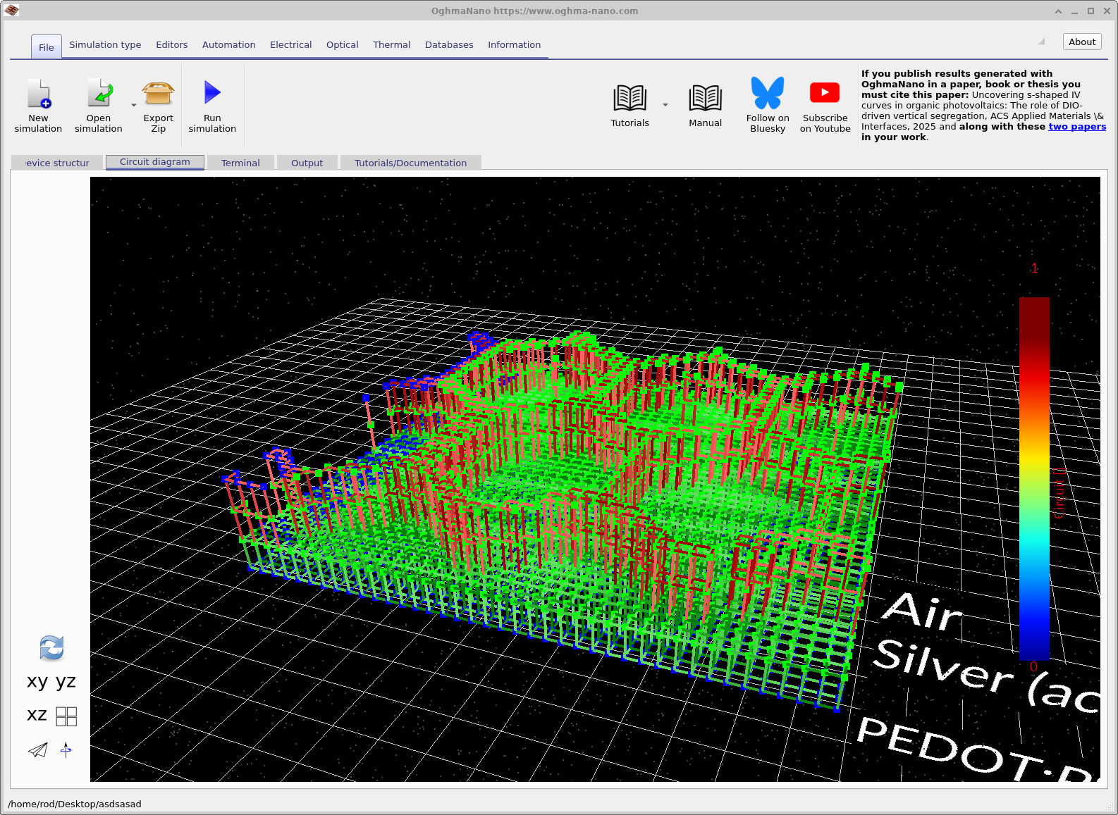
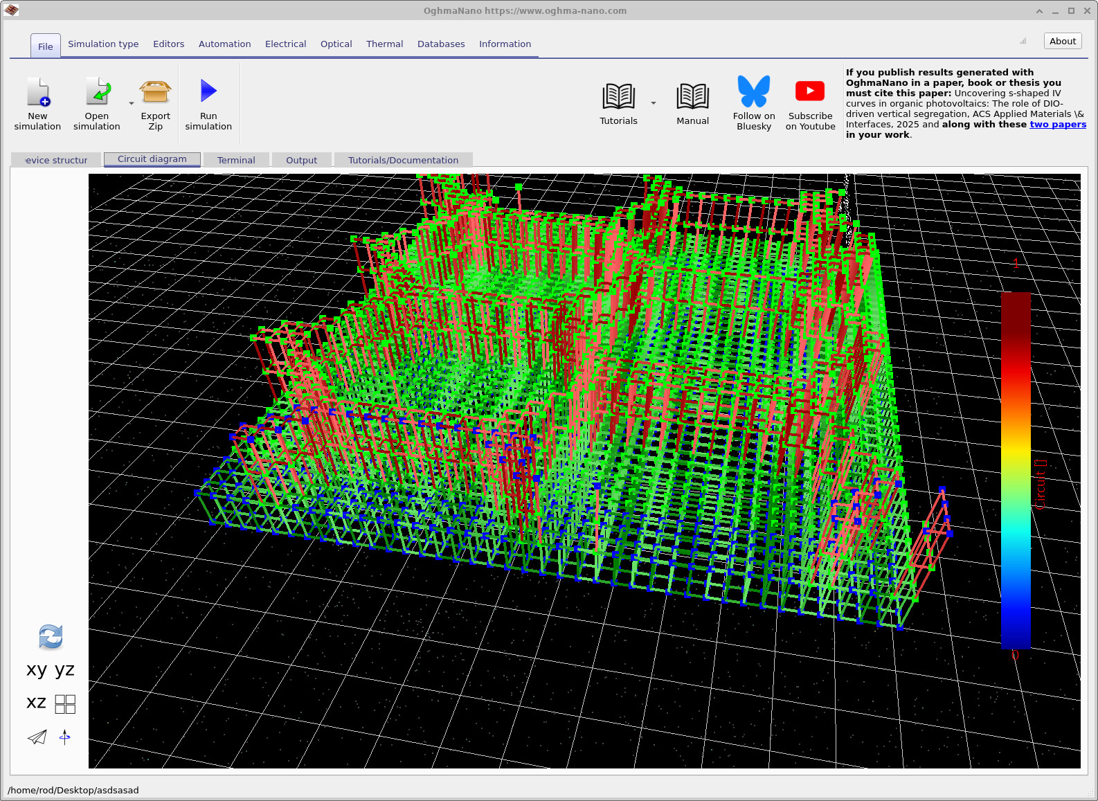
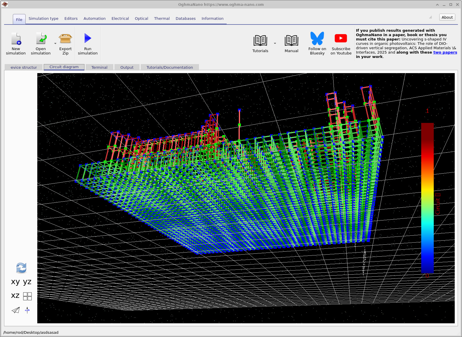
In this view, each link corresponds to a resistor, and each green node represents a circuit node. Blue nodes indicate points where current is extracted from the structure. The yellow extraction bar seen earlier defines which regions act as electrical exits. Flipping the structure reveals that the bottom surface also contains extraction nodes, corresponding to the lower contact.
At this point, the simulation geometry and circuit representation are fully defined. In the next part of the tutorial, we will apply voltages, run the solver, and quantify resistive losses and voltage drops across the contact.
👉 Next step: Continue to Part B to run the simulation and analyse current flow and voltage loss.