Polycrystalline Silicon Solar Cell (1D) — Industrial n+/p/p+ (Al-BSF-class)
1. Introduction

Polycrystalline silicon solar cells have played a central role in the development of the global photovoltaic industry and remain widely deployed, particularly in large-area and cost-sensitive applications such as utility-scale solar farms (see ??). Although recent manufacturing trends have favoured monocrystalline formats, polycrystalline silicon devices remain an important reference technology with well-understood performance limits and loss mechanisms.
This tutorial provides a practical, physics-based workflow for simulating a silicon solar cell in 1D using OghmaNano. The model resolves drift–diffusion carrier transport coupled to Poisson electrostatics, with depth-dependent optical generation and physically motivated recombination (Shockley–Read–Hall and Auger). The goal is to connect standard outputs—JV curves, Voc, and Suns–Voc behaviour—to the underlying internal variables (bands, quasi-Fermi levels, charge, and recombination time).
You will construct and simulate a one-dimensional polycrystalline silicon solar cell with an industrial n+/p/p+ aluminium back-surface field (Al-BSF) architecture (see ??). The device is defined as: Structure (front → back): n+ Si / p Si / p+ Si / Al. Using this baseline device, you will generate an illuminated JV curve, extract key performance metrics, and run Voc and Suns–Voc sweeps to identify recombination-limited voltage loss and its dependence on carrier density.
2. Making a New Simulation
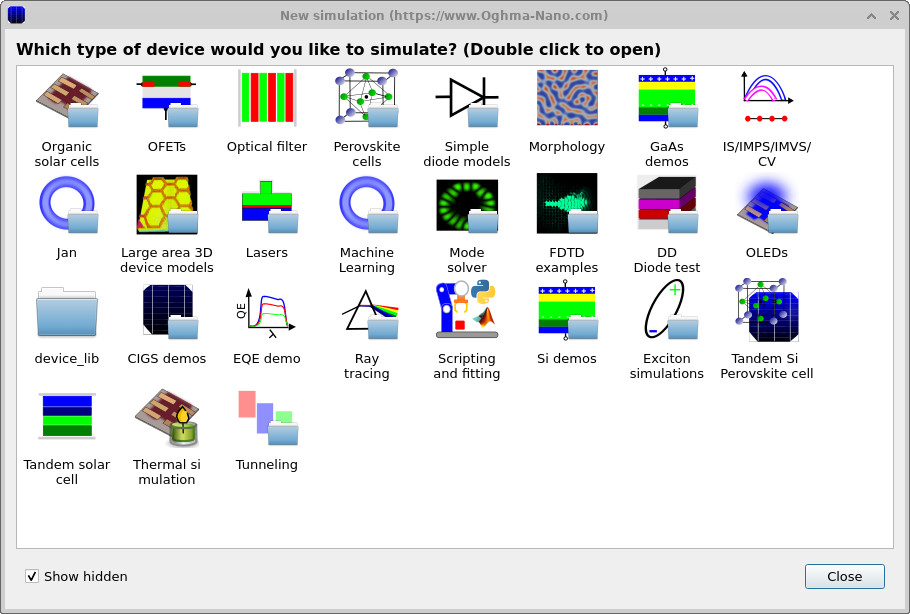
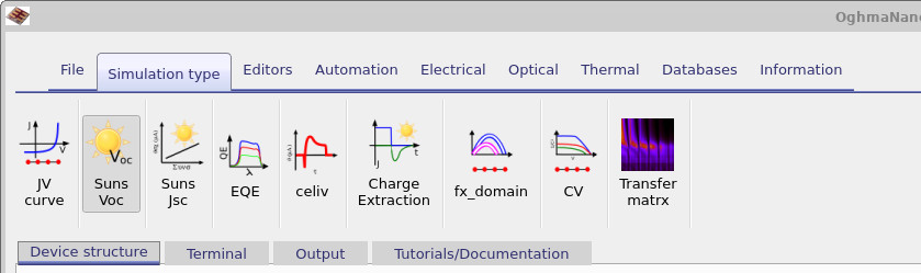
To begin, create a new simulation from the main OghmaNano window. Click on the New simulation button in the toolbar. This opens the simulation-type selection dialog (see ??).
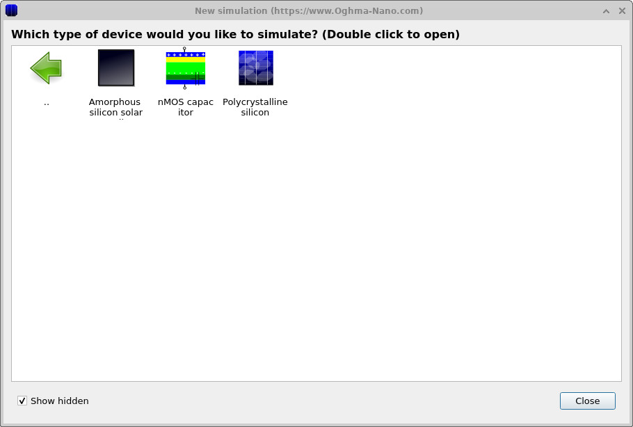
In the simulation-type dialog, double-click on Si demos, then double-click on Polycrystalline silicon (see ??). OghmaNano will load a predefined polycrystalline silicon solar-cell simulation.
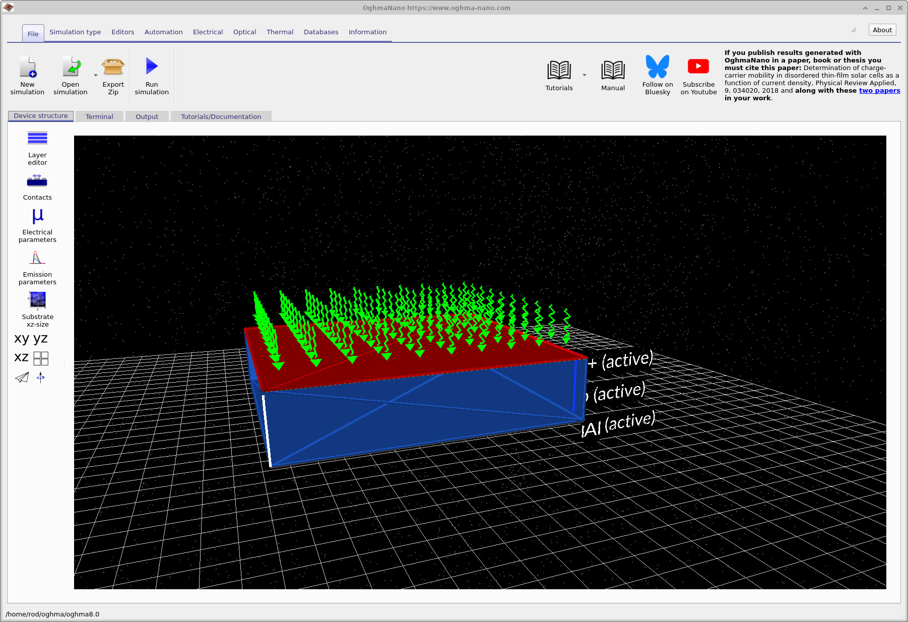
The main window (see ??) provides a three-dimensional view of the device structure. You can use the mouse to rotate, pan, and zoom the scene to inspect the geometry. Although the present tutorial uses a one-dimensional electrical model, the 3D view provides a convenient way to visualise the layer stack and contacts.
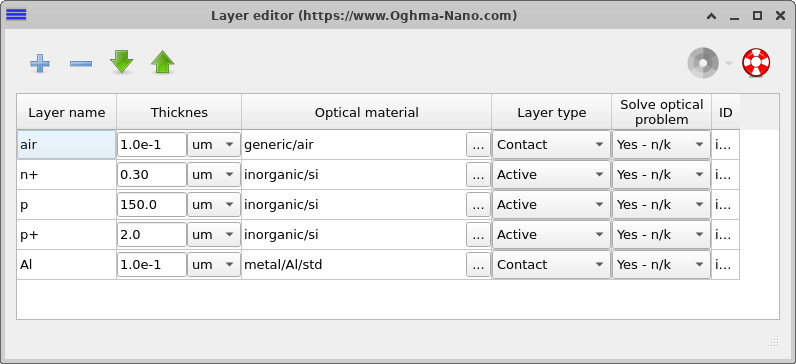
Click on the Layer editor tab to open the layer table (see ??). Here you can inspect the vertical device structure, including the n+ emitter, p-type base, p+ back-surface field, and aluminium back contact, along with their thicknesses and assigned materials.
3. Examining the doping profile
The doping profile sets the electrostatic landscape of the device before illumination and bias are applied. In practice it determines where the p–n junction sits, how wide the depletion region is, and the magnitude of the built-in electric field that separates photogenerated carriers. For an industrial silicon solar cell, doping is also used strategically to control recombination at the contacts: heavily doped surface regions are introduced to form selective junctions and to reduce minority-carrier losses near metals.
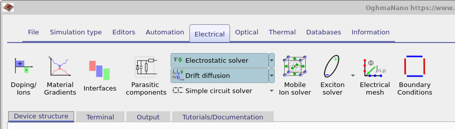
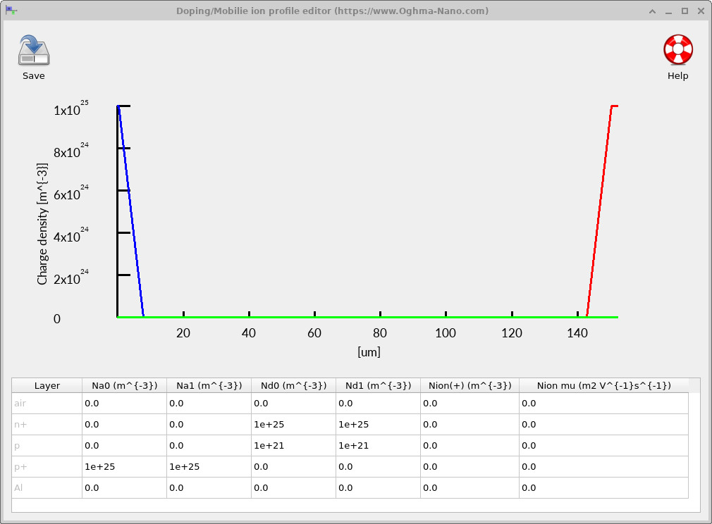
To view the doping in OghmaNano, go to the Electrical ribbon in the main window and click Doping / Ions (see ??). This opens the profile editor (see ??), which plots charge density versus depth and lists the numerical donor and acceptor densities assigned to each layer.
The device uses a standard n+/base/p+ polycrystalline silicon doping profile. At the illuminated front surface, a thin n+ emitter is introduced with a very high donor concentration (peaking at \(\sim 10^{25}\,\mathrm{m^{-3}}\)), confined to the first few microns of the structure. This heavily doped region establishes a strong near-surface electric field and provides an ohmic, electron-selective contact for efficient carrier extraction. The emitter concentration then drops sharply into the bulk of the device. The central region of the structure is the thick silicon absorber (the base), which is doped several orders of magnitude more lightly (here \(\sim 10^{21}\,\mathrm{m^{-3}}\)). This region provides the main volume for optical absorption and carrier transport while maintaining moderate resistivity and limiting space-charge effects away from the contacts. At the rear of the device, a thin p+ layer adjacent to the aluminium contact is heavily acceptor-doped (again \(\sim 10^{25}\,\mathrm{m^{-3}}\)), forming a back-surface field. The p+ back-surface field shapes the band bending near the rear contact, repels minority carriers from the metal interface, and suppresses rear-contact recombination, thereby improving carrier collection and preserving open-circuit voltage.
4. Electrical parameters: transport, electrostatics, and recombination
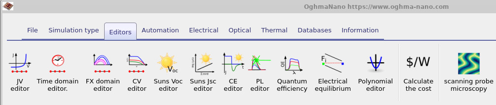
Open the electrical parameter editor from the main window: Device structure → Electrical parameters. Parameters are defined per region using the n+, p, and p+ tabs (emitter, base, and back-surface field respectively). The settings in this editor determine the drift–diffusion transport coefficients, the energetic alignment, and the recombination mechanisms used during the JV sweep.
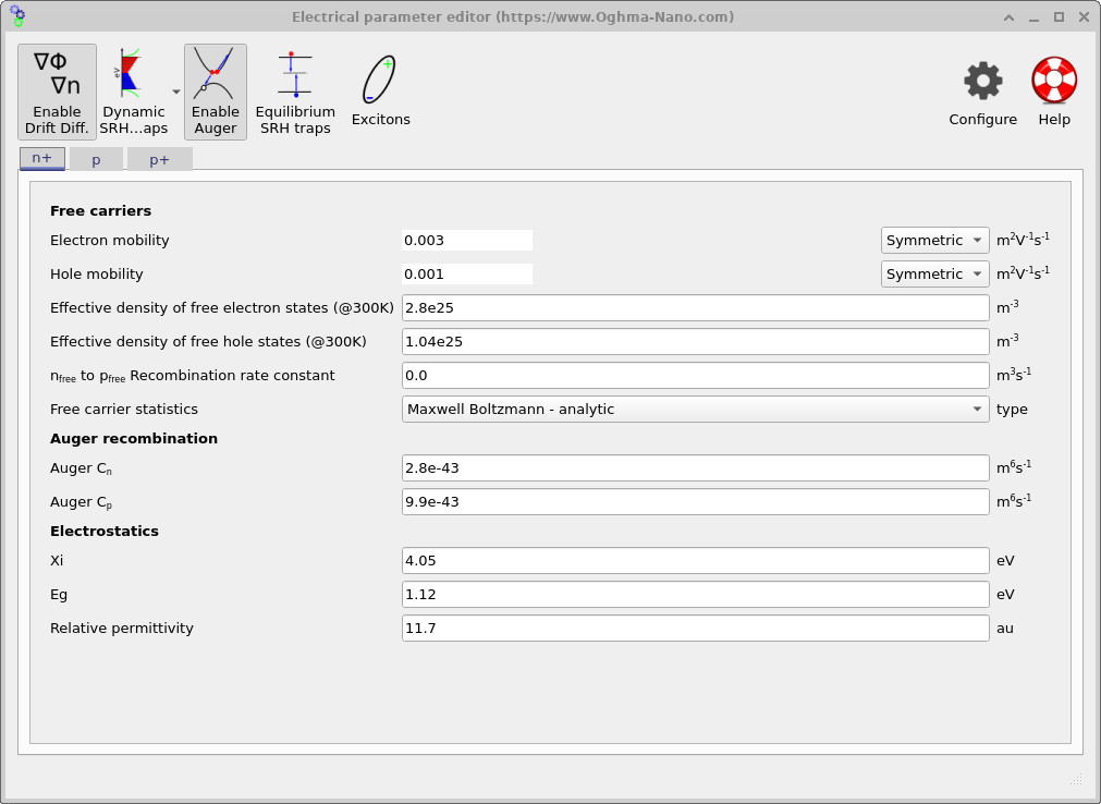
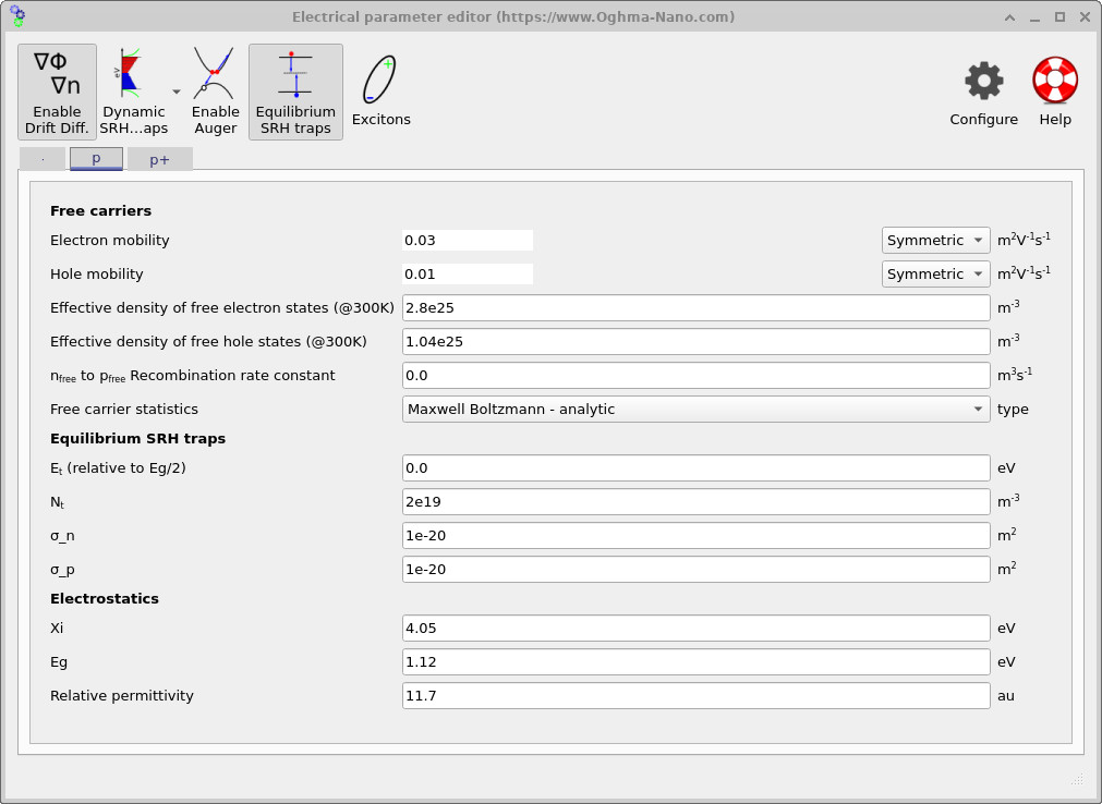

Transport in each region is set by the electron and hole mobilities. In the p base (see ??), the mobilities are set to μn = 0.03 m2V-1s-1 and μp = 0.01 m2V-1s-1, providing efficient transport through the thick absorber. In the heavily doped n+ and p+ regions (see ?? and ??), the mobilities are set lower (μn = 0.003, μp = 0.001 m2V-1s-1) to represent the reduced carrier mobility typically associated with heavily doped/polycrystalline contact regions. These values affect the series-resistance contribution at high current and the local carrier gradients required to sustain extraction.
The effective densities of states Nc = 2.8×1025 m-3 and Nv = 1.04×1025 m-3 (visible in each tab). Together with the bandgap, these parameters set the intrinsic carrier density and the equilibrium carrier populations. Electrostatics are defined by the electron affinity χ = 4.05 eV, bandgap Eg = 1.12 eV, and relative permittivity εr = 11.7, consistent with silicon at room temperature. These values define the band-edge reference, depletion behaviour, and the built-in field that arises when combined with the doping profile.
Recombination is enabled on a per-region basis. In the heavily doped n+ emitter and p+ BSF, Auger recombination is enabled (Auger button depressed in ?? and ??), with coefficients Cn = 2.8×10-43 m6s-1 and Cp = 9.9×10-43 m6s-1. Auger recombination captures the dominant high-density loss mechanism in these regions; a common form is \[ R_{\mathrm{Auger}} = C_n\,n^2 p + C_p\,p^2 n, \] so the rate increases rapidly when carrier concentrations are large, as they are in heavily doped contact-adjacent layers under injection. Including Auger loss here prevents unphysical carrier pile-up at the contacts and yields realistic voltage and current behaviour when the device is driven to high injection.
In the p base, recombination is treated as lifetime-limited by Shockley–Read–Hall (SRH) traps using the Equilibrium SRH traps model (enabled in ??). The trap energy is set at mid-gap (Et relative to Eg/2 = 0), with trap density Nt = 2×10¹⁹ m-3 and capture cross-sections σn = σp = 1×10-20 m2. In this equilibrium formulation, the capture cross-sections determine the carrier capture coefficients \(c_n = \sigma_n v_{\mathrm{th}}\) and \(c_p = \sigma_p v_{\mathrm{th}}\), where \(v_{\mathrm{th}}\) is the thermal velocity. The corresponding electron and hole lifetimes are therefore \[ \tau_n = \frac{1}{\sigma_n v_{\mathrm{th}} N_t}, \qquad \tau_p = \frac{1}{\sigma_p v_{\mathrm{th}} N_t}, \] linking the GUI parameters directly to the effective bulk lifetime. The resulting SRH recombination rate takes the standard form \[ R_{\mathrm{SRH}} = \frac{np - n_i^2}{\tau_p (n+n_1) + \tau_n (p+p_1)}, \] where \(n_1\) and \(p_1\) are set by the trap energy level \(E_t\). Since the bulk generates most of the photocurrent, SRH recombination in the base is the primary mechanism controlling Voc in this tutorial, while Auger losses are confined mainly to the heavily doped surface regions. A detailed discussion of SRH theory is given in Shockley–Read–Hall recombination, the physical motivation for including traps in Why traps are required, and the fully non-equilibrium formulation in Dynamic (non-equilibrium) SRH modelling.
5. Optical generation profile
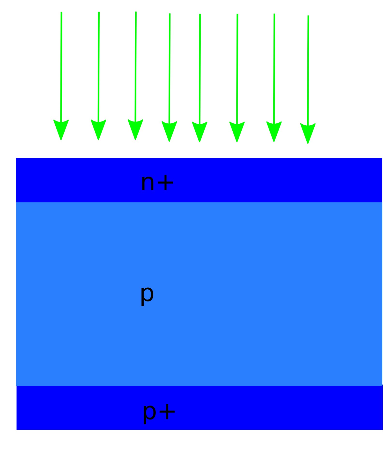
This demo uses a one-dimensional optical calculation to generate a depth-dependent source term for the drift–diffusion solver. In practice, the optical model computes how the incident AM1.5 spectrum propagates into the silicon, how much is absorbed as a function of wavelength and depth, and converts that absorbed power into an electron–hole pair generation rate. In a silicon solar cell the optical profile largely fixes Jsc, while Voc is then set by the balance of generation and recombination.
To view (and regenerate) the optical solution, go to the Optical ribbon in the main window and click Transfer matrix. This opens the optical simulation editor. Press the blue Run optical simulation button (the play icon) to calculate the optical field and update the plots (see ??).
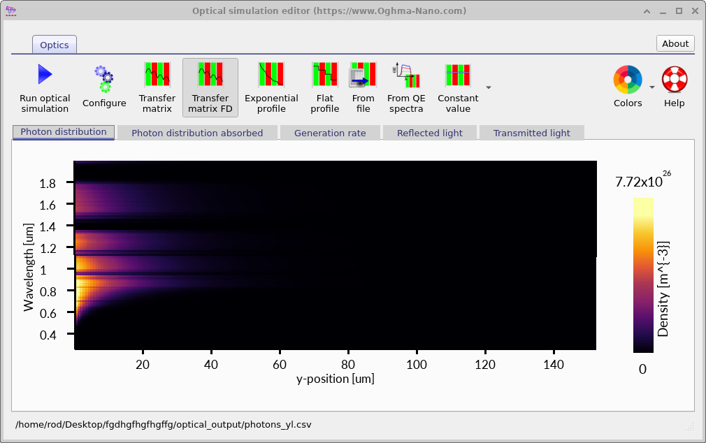
The plot in ?? is a wavelength–depth map. The horizontal axis is depth into the device (labelled y-position), and the vertical axis is wavelength. Bright colours near the illuminated surface indicate a high photon population; the rapid fading with depth shows that light is being absorbed as it propagates into the silicon.
For polycrystalline silicon this front-loaded behaviour is expected. Silicon absorbs strongly at shorter wavelengths, so blue/visible photons are depleted very quickly near the front surface, while longer wavelengths penetrate further before being absorbed. You should therefore read the map from bottom to top: short wavelengths die out near the front; longer wavelengths extend deeper. At wavelengths beyond roughly 1.1 µm the photon energy is below the silicon bandgap, so those photons do not drive band-to-band carrier generation and contribute little to photovoltaic current even if they are present in the spectrum.
The optical editor provides several tabs because “photon density” is not the same thing as “generation rate”. The Photon distribution view (shown above) tells you where the optical field exists. The Photon distribution absorbed and Generation rate tabs are the ones that matter for the electrical model: the absorbed photon map is converted into a depth-dependent electron–hole pair generation rate, which is the source term injected into the drift–diffusion equations. For this cell, the resulting generation profile peaks near the front and decays into the base, consistent with a front-illuminated n+/p junction device.
6. Running the simulation, JV curves, and extracting parameters
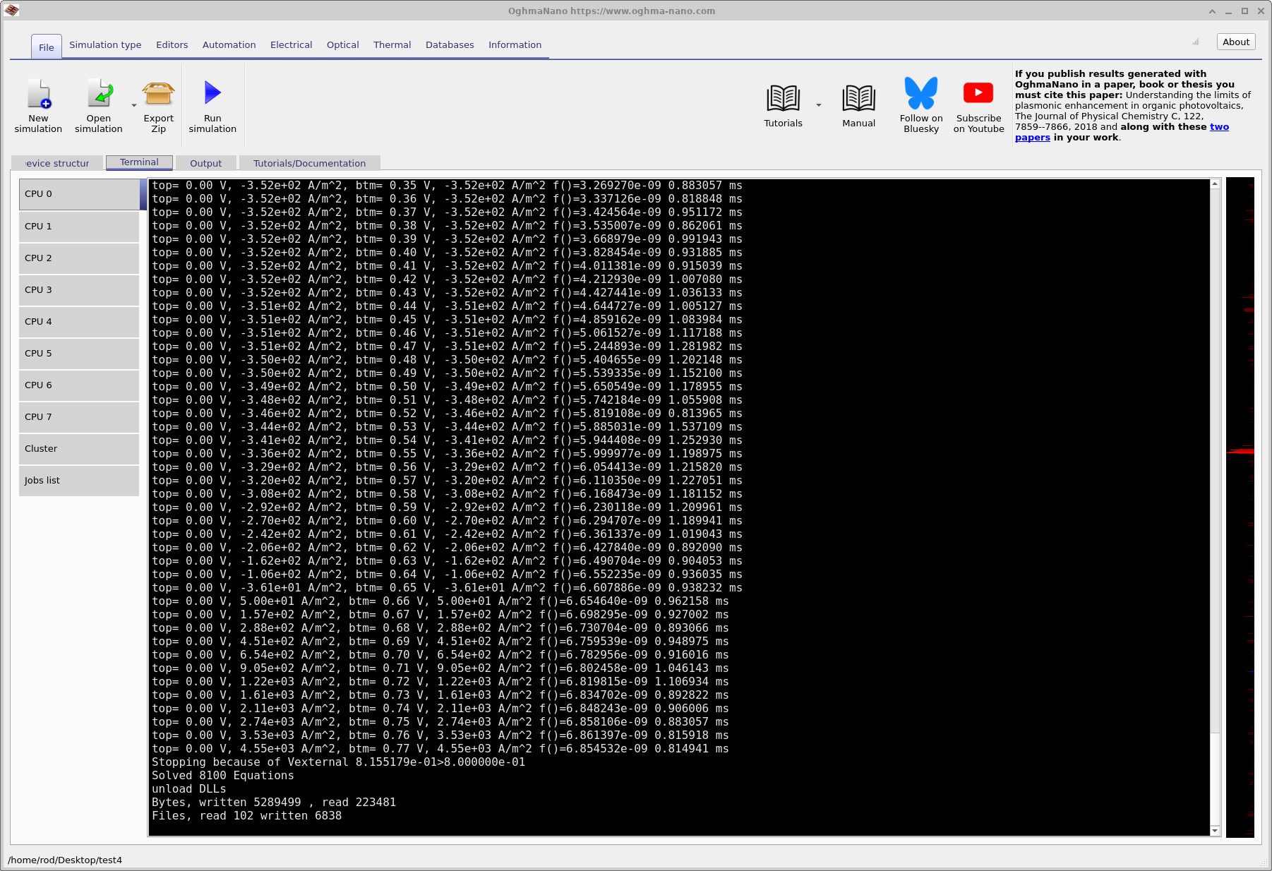
Once the device structure, electrical parameters, and optical generation are defined, the simulation can be run directly from the main window. Click the Run simulation button in the toolbar to start the solver. During execution, solver progress and convergence information are written to the terminal window (see ??).
Although the terminal output appears verbose, it follows a clear structure. For each bias point, the applied voltage at the top contact is listed first, followed by the resulting current density. Under illumination the current is initially negative, indicating power generation. As the applied voltage is increased, the current magnitude decreases until it crosses zero at the open-circuit voltage. Beyond this point the current becomes positive, corresponding to forward-biased diode operation. The terminal output also reports the voltage and current at the bottom contact, the solver residual (error), and the time taken to converge each bias step. Small residuals indicate that the coupled drift–diffusion and Poisson equations are being solved accurately.
jv.csv and siminfo.dat.
jv.csv. The curve shows negative current at low voltage,
a zero-current crossing at Voc, and forward conduction at higher bias.
siminfo.dat, listing extracted device metrics
such as Voc, Jsc, fill factor, and efficiency.
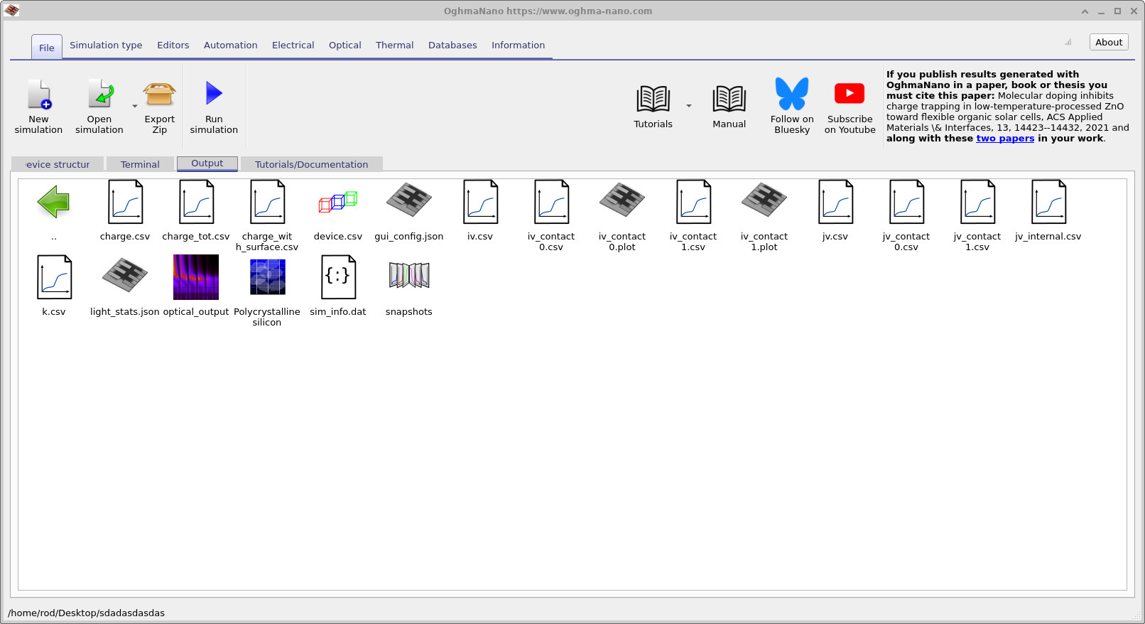
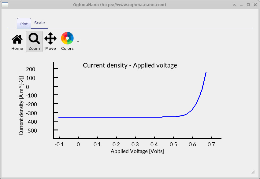
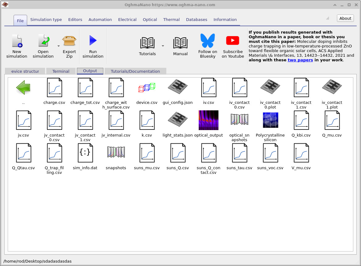
To inspect the electrical characteristics, open the Output tab and double-click
jv.csv. This displays the current density–voltage (JV) curve
(see ??).
The JV curve is the primary diagnostic of device behaviour: it should pass through the short-circuit current
at zero bias and cross zero current at the open-circuit voltage.
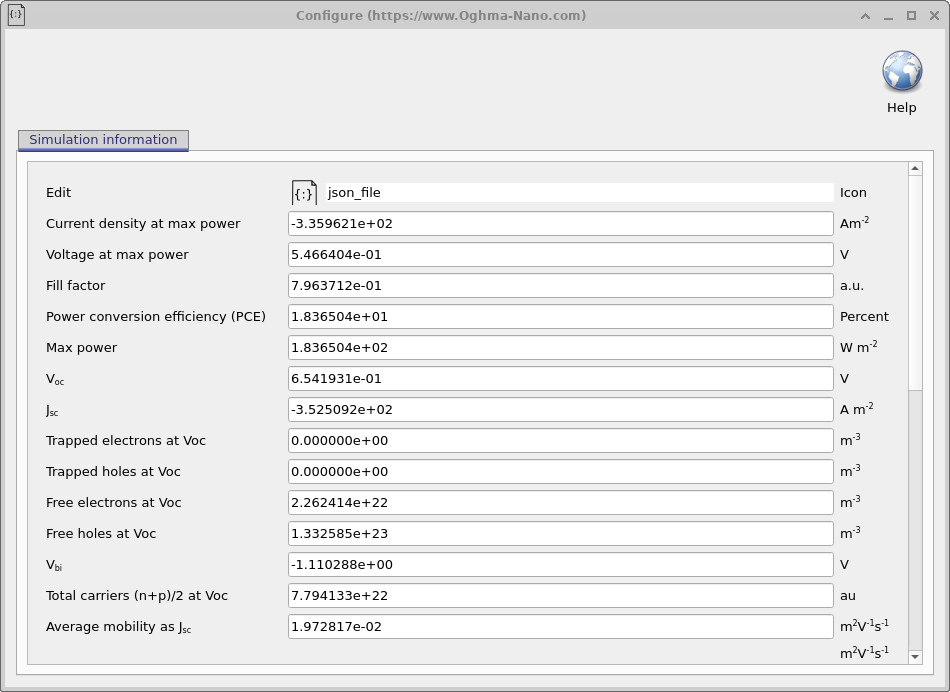
Double-clicking siminfo.dat opens the simulation information window
(see ??),
which reports the extracted performance metrics, including fill factor, power conversion efficiency,
maximum power point, Voc, and Jsc.
Additional diagnostic quantities, such as free carrier densities at open circuit, are also listed and are
useful for interpreting recombination-limited behaviour.
A practical rule is to always inspect the JV curve before interpreting the numerical metrics.
If the JV curve does not pass cleanly through short circuit and open circuit, or if the current has an
unexpected sign or shape, the derived quantities in siminfo.dat will also be unreliable.
In practice, visual inspection of the JV curve is the fastest way to diagnose configuration or modelling issues.
7. Examining internal snapshots: bands and quasi-Fermi levels
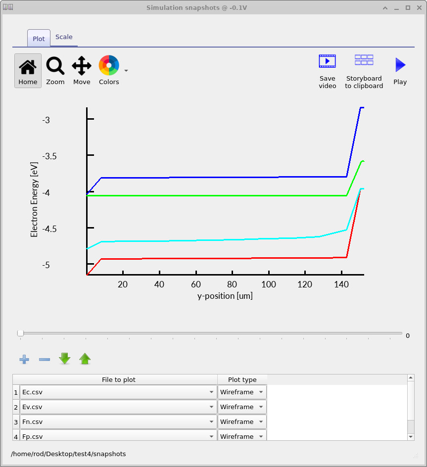
During a JV sweep, OghmaNano saves the full internal solution at each bias point into the snapshots directory. These snapshot files contain the internal state of the device—band edges, quasi-Fermi levels, carrier densities, currents, and related quantities—and are the most direct way to verify what the solver is doing inside the structure rather than inferring behaviour only from the JV curve.
Open the Output tab, locate the snapshots folder, and double-click it to launch the snapshot viewer. The viewer is an interactive plotting window which can overlay multiple internal variables on the same axes and allows you to step through the saved bias points using the voltage slider.
To reproduce the band/quasi-Fermi plot used in this tutorial, add four traces using the + button.
Under File to plot, select (in order) Ec.csv, Ev.csv, Fn.csv, and Fp.csv.
These correspond to the conduction band edge (Ec), valence band edge (Ev),
electron quasi-Fermi level (Fn), and hole quasi-Fermi level (Fp).
Ec, Ev, Fn, and Fp.
Ec, Ev, Fn, and Fp.
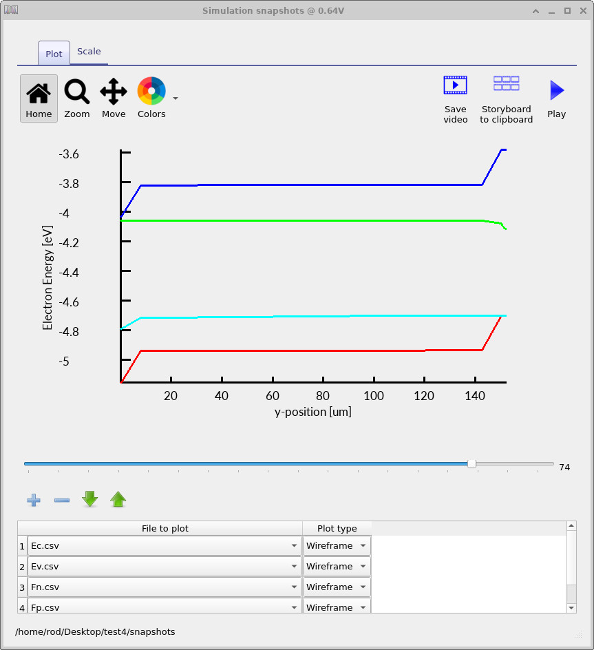
Use the voltage slider to move through the JV sweep from short circuit to open circuit and observe how the internal energies evolve as the extracted current is reduced. At short circuit (see ??), the device operates in a current-extracting regime: photogenerated carriers are removed through the selective contacts and a finite transport driving force must be sustained. In drift–diffusion form, the electron and hole currents are given by \[ J_n = \frac{\sigma_n}{q}\,\nabla E_{Fn}, \qquad J_p = -\frac{\sigma_p}{q}\,\nabla E_{Fp}, \] so a non-zero terminal current requires a spatial gradient in at least one of the quasi-Fermi levels. In selectively contacted structures, this gradient need not be shared equally: one quasi-Fermi level may remain relatively flat (for example, if it is strongly pinned by an ohmic majority-carrier contact) while the other carries most of the transport-driving variation. The band edges themselves are not required to be flat and typically exhibit pronounced bending near heavily doped regions and contacts.
As the applied voltage is increased toward open circuit, the net terminal current decreases and the solution
approaches a zero-current steady state. In the device interior, the quasi-Fermi levels become approximately flat
because both electron and hole currents vanish,
\[
J_n \approx 0, \qquad J_p \approx 0,
\]
while the conduction and valence band edges generally remain bent due to built-in electrostatics arising from
doping gradients, space charge, and contact selectivity. In selectively contacted devices, small deviations from
perfect quasi-Fermi-level flatness may persist within narrow boundary layers adjacent to carrier-blocking contacts;
these reflect zero-flux boundary conditions on the blocked carrier species rather than current flow. At open circuit
(see ??),
photogeneration is balanced by recombination throughout the device, and the separation between the electron and hole
quasi-Fermi levels in the bulk,
\[
qV_{\mathrm{oc}} = E_{Fn} - E_{Fp},
\]
is the microscopic origin of the open-circuit voltage reported in siminfo.dat. When stepping from short
circuit to open circuit using the slider, the key signature to look for is the relaxation of transport-driving
gradients in the device interior while the quasi-Fermi-level splitting persists.
8. Suns–Voc curves
Suns–Voc measurements probe how the open-circuit voltage evolves with illumination intensity. Because Voc is set by the separation of the electron and hole quasi-Fermi levels, its dependence on light intensity provides direct insight into the dominant recombination mechanisms in the device. In principle, a Suns–Voc curve can be constructed by running a large number of illuminated JV sweeps and extracting Voc at each intensity. Rather than constructing a sequence of JV curves and extracting Voc manually, OghmaNano provides a dedicated Suns–Voc simulation mode. To enable this, open the Simulation type ribbon in the main window (see ??) and select Suns–Voc. This switches the solver from a voltage sweep to an intensity sweep carried out explicitly at open circuit.
After selecting Suns–Voc, click Run simulation.
For each illumination level, the solver adjusts the terminal voltage until the
net current is zero, thereby computing the open-circuit operating point directly.
The resulting data are written to disk automatically and can be inspected from
the Output tab. Among the generated files is suns_voc.csv, which contains the open-circuit
voltage as a function of light intensity.
Double-clicking this file opens the Voc–intensity plot shown in
??.
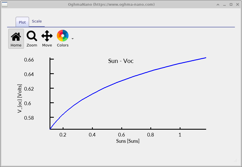
At low illumination, Voc increases rapidly with light intensity, consistent with the logarithmic dependence of quasi-Fermi level separation on carrier density. As the illumination level rises, the slope of the Voc–intensity curve decreases, signalling that recombination is increasingly limiting further voltage gain. To expose this transition more clearly, extend the illumination range to higher intensity. Open the Suns–Voc editor from the Editors ribbon and increase the stop intensity from 1.1 to 100 suns, then rerun the simulation.
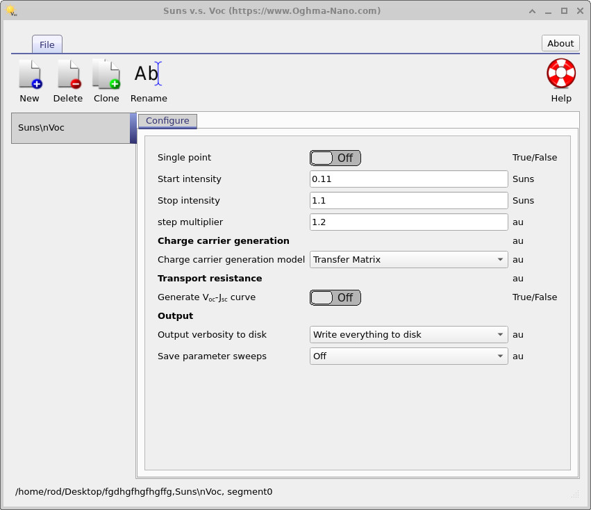
Rerun the simulation and open suns_voc.csv again.
The extended illumination range reveals the high-intensity behaviour of Voc.
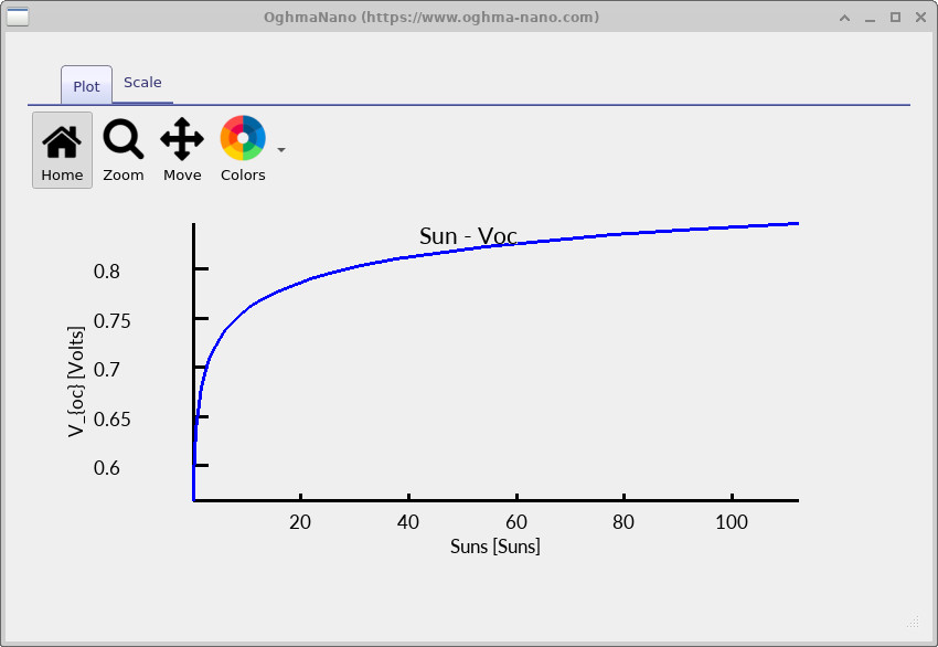
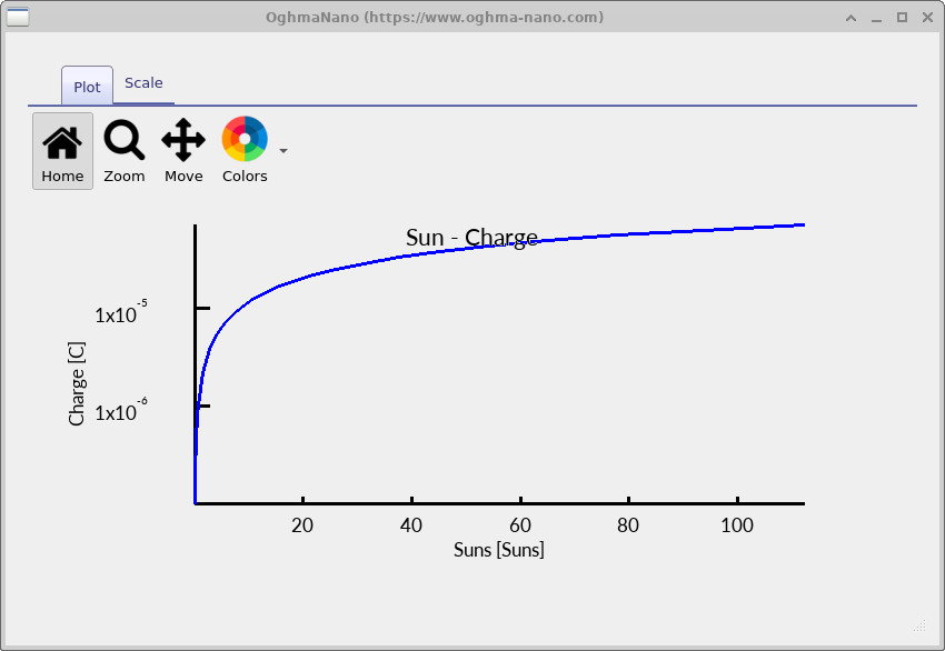
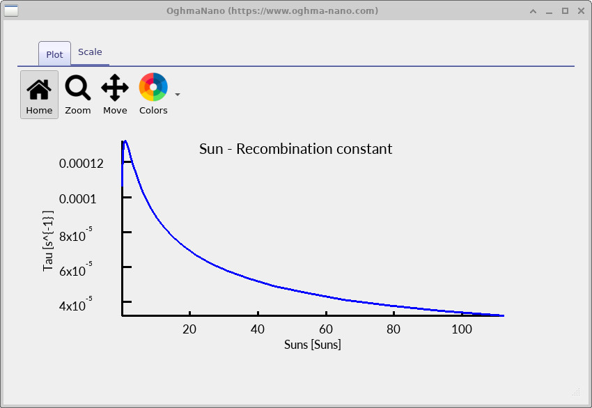
As the illumination level increases, the total excess carrier density in the device rises. Under open-circuit conditions this charge must recombine locally, so the steady-state recombination rate increases with carrier density. For band-to-band and defect-assisted recombination processes, the recombination rate scales approximately as R ∝ n p, while Auger recombination introduces an additional high-density term RAuger ∝ n2p + np2. As a result, the effective carrier lifetime τeff = Δn / R decreases as illumination increases.
The open-circuit voltage is set by the quasi-Fermi level splitting, qVoc = EFn - EFp , which for a non-degenerate semiconductor can be written as Voc = (kT/q) ln(n p / ni2) . Increasing illumination raises the carrier density and therefore increases Voc, but only logarithmically. Once recombination accelerates sufficiently, further increases in carrier density produce diminishing gains in quasi-Fermi level separation.
This competition between generation and recombination causes Voc to saturate at high illumination. The maximum voltage remains below the silicon bandgap (Eg = 1.12 eV), because recombination prevents the electron and hole quasi-Fermi levels from reaching the band edges simultaneously. The difference Eg/q − Voc therefore represents the intrinsic voltage loss imposed by recombination under high-injection conditions for this device.