Amorphous Silicon (a-Si:H) Solar Cell (1D) — Thin-Film p/i/n (Defect-limited)
1. Introduction

Hydrogenated amorphous silicon (a-Si:H) solar cells are a canonical thin-film photovoltaic technology. Unlike crystalline silicon, a-Si:H is structurally disordered and contains a high density of defect and tail states. As a result, device behaviour is typically recombination-limited by defects (Shockley–Read–Hall-type processes) and transport-limited by lower mobilities. This makes a-Si:H an excellent system for learning how recombination and carrier density determine Voc, and how thin-film optics shapes Jsc.
This tutorial provides a practical, physics-based workflow for simulating an a-Si:H solar cell in 1D using OghmaNano. The model resolves drift–diffusion carrier transport coupled to Poisson electrostatics, with depth-dependent optical generation and physically motivated recombination dominated by SRH-type defect recombination. The goal is to connect standard outputs—JV curves, Voc, and Suns–Voc behaviour—to internal variables (bands, quasi-Fermi levels, charge, and effective recombination time).
You will construct and simulate a one-dimensional thin-film a-Si:H solar cell with a standard p/i/n architecture (see ??). The device is defined as: Structure (front → back): p a-Si:H / i a-Si:H / n a-Si:H / metal contact. Using this baseline device, you will generate an illuminated JV curve, extract key performance metrics, and run Voc and Suns–Voc sweeps to identify recombination-limited voltage loss and its dependence on carrier density.
2. Making a New Simulation
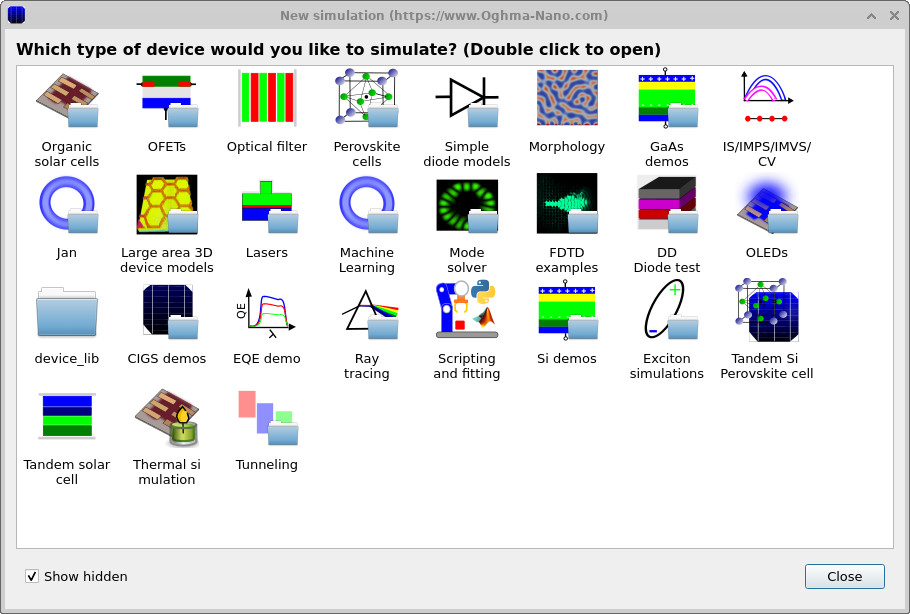
To begin, create a new simulation from the main OghmaNano window. Click on the New simulation button in the toolbar. This opens the simulation-type selection dialog (see ??).
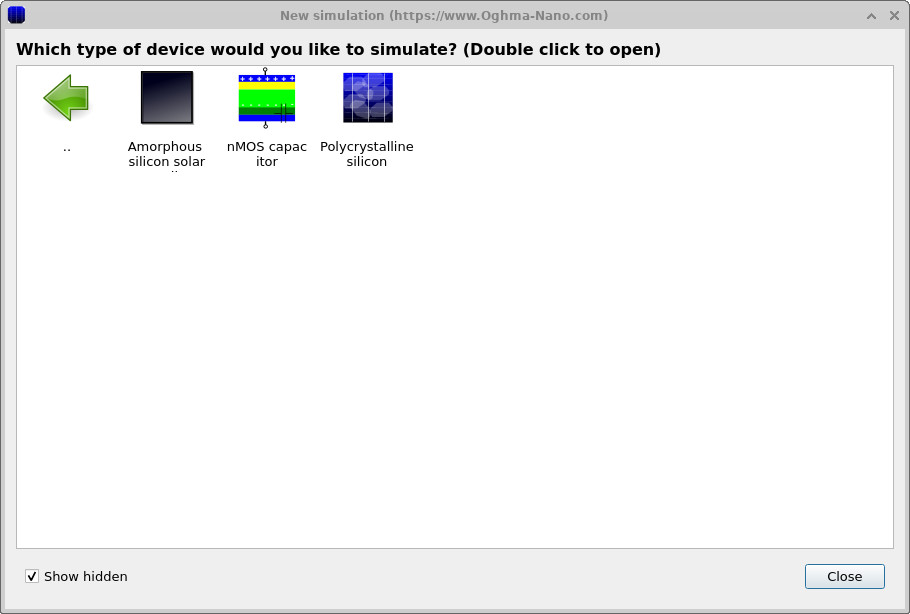
In the simulation-type dialog, double-click on Si demos, then double-click on Amorphous silicon (a-Si:H) (see ??). OghmaNano will load a predefined a-Si:H thin-film solar-cell simulation.
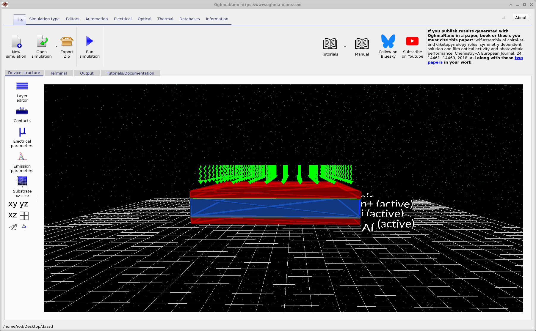
The main window (see ??) provides a three-dimensional view of the device structure. You can use the mouse to rotate, pan, and zoom the scene to inspect the geometry. Although the present tutorial uses a one-dimensional electrical model, the 3D view provides a convenient way to visualise the thin-film stack and contacts.
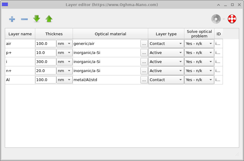
Click on the Layer editor tab to open the layer table (see ??). Here you can inspect the vertical device structure, including the p-type layer, intrinsic absorber (i-layer), n-type layer, and the back contact, along with their thicknesses and assigned materials.
3. Examining the doping profile
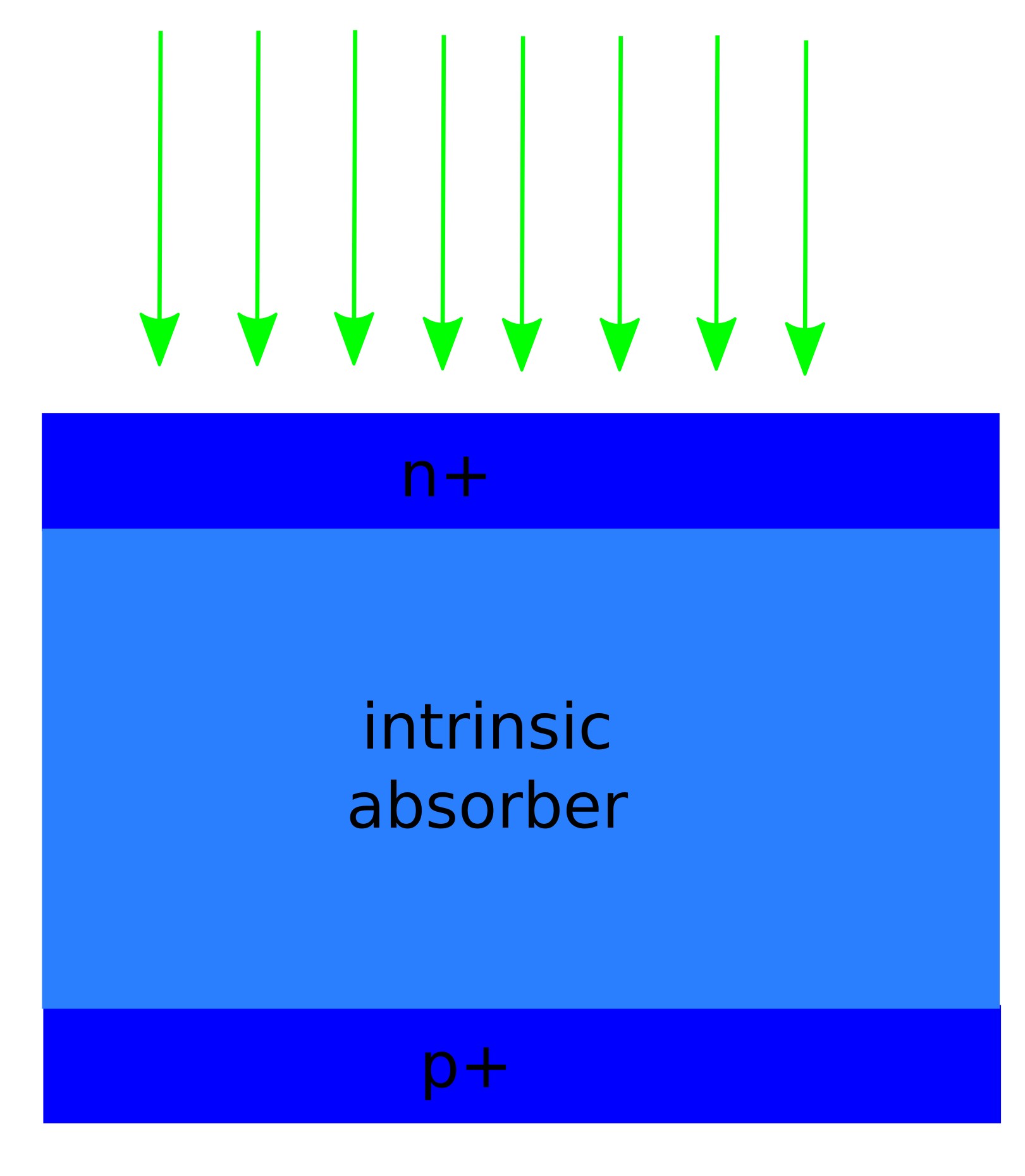
The doping profile sets the electrostatic structure of the device before illumination and bias are applied. In a thin-film amorphous silicon (a-Si:H) solar cell, doping is used primarily to form carrier-selective contacts rather than to create a wide depletion region inside a doped absorber. The central operating principle is the built-in electric field across an intrinsic layer, which separates and transports photogenerated carriers.
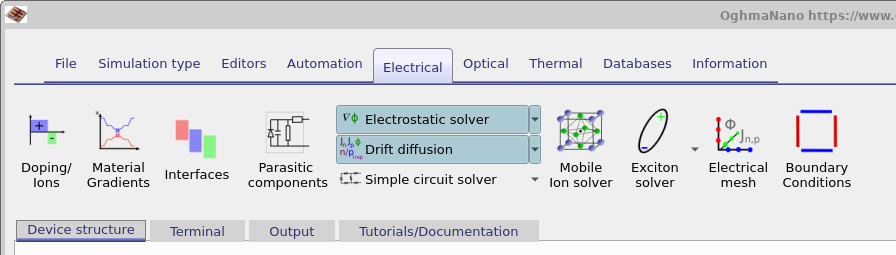
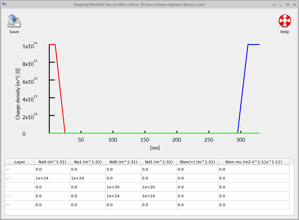
To view the doping in OghmaNano, open the Electrical ribbon in the main window and click Doping / Ions (see ??). This opens the profile editor (see ??), which plots donor and acceptor charge density versus depth and lists the numerical values assigned to each layer.
The device uses a standard p+/i/n+ a-Si:H architecture. A thin, heavily doped p+ layer is placed at the illuminated front surface (acceptor density on the order of \(10^{24}\,\mathrm{m^{-3}}\)), providing a hole-selective contact and setting the front-side band bending. This is followed by a much thicker intrinsic a-Si:H absorber layer, which is only very lightly doped (here \(\sim 10^{20}\,\mathrm{m^{-3}}\)) and contains the majority of the optical generation. At the rear of the device, a thin, heavily doped n+ layer (donor density again \(\sim 10^{24}\,\mathrm{m^{-3}}\)) forms an electron-selective back contact adjacent to the metal.
The key feature to recognise in the profile editor is that the strong built-in electric field spans the intrinsic layer, not the doped regions. Photogenerated carriers are created primarily in the intrinsic a-Si:H and are separated by this internal field: electrons are driven toward the n+ back contact, while holes are driven toward the p+ front contact. The doped layers are kept thin to minimise defect-assisted recombination, while still providing good electrical selectivity and contact conductivity.
4. Electrical parameters: transport, electrostatics, and recombination in a-Si:H
Open the electrical parameter editor from the main window: Device structure → Electrical parameters. Parameters are defined per region using the p+, i, and n+ tabs, corresponding to the front contact layer, intrinsic absorber, and back contact layer of the a-Si:H stack. The settings in this editor determine the drift–diffusion transport coefficients, the energetic alignment, and the recombination mechanisms used during JV and Suns–Voc sweeps.
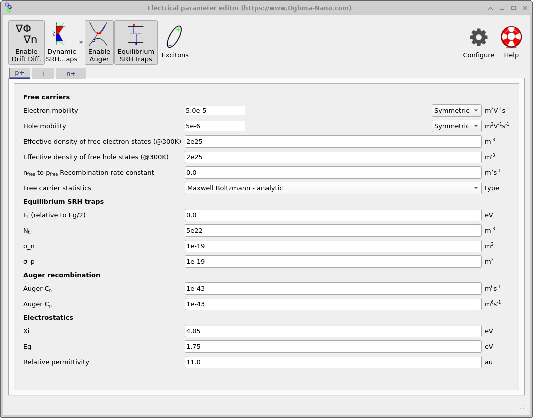
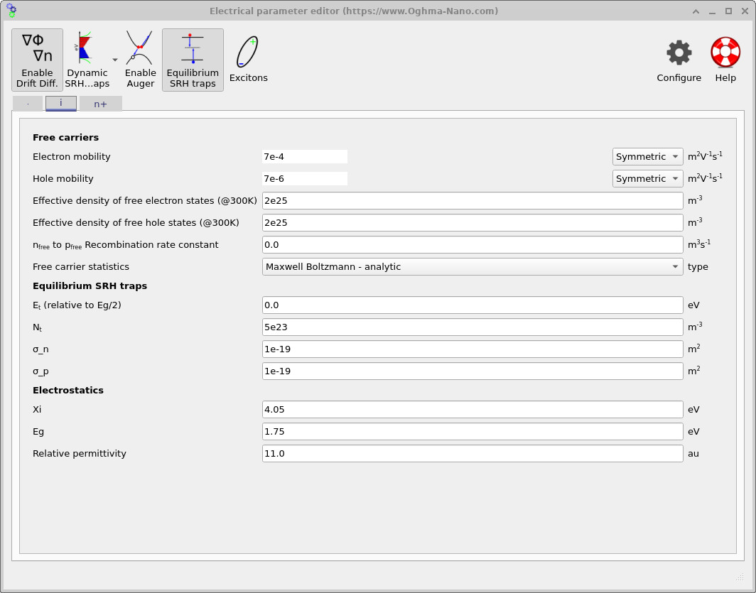
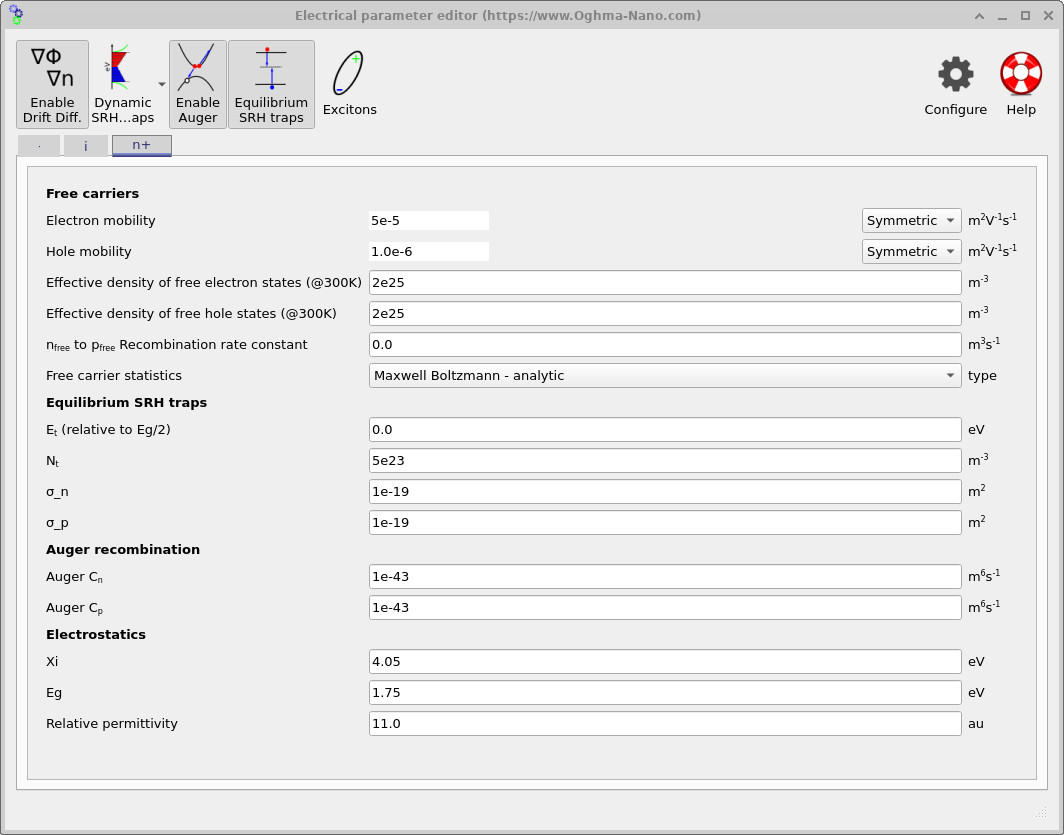
Transport in amorphous silicon is characterised by low mobilities due to disorder and strong scattering. The demo therefore uses mobilities far below crystalline silicon. In the intrinsic layer (see ??), the electron mobility is set to μn = 7×10⁻⁴ m2V−1s−1 and the hole mobility to μp = 7×10⁻⁶ m2V−1s−1. The contact-adjacent layers use different (typically lower) mobilities (see ?? and ??), reflecting the fact that the doped/selective layers act primarily as thin extraction regions rather than high-mobility absorbers. In drift–diffusion, reduced mobility increases the carrier residence time and makes recombination more consequential near open circuit.
The electrostatic baseline used throughout the stack is visible in every tab: electron affinity χ = 4.05 eV, bandgap Eg = 1.75 eV, and relative permittivity εr = 11. The wider bandgap reflects the optical gap of a-Si:H and sets the upper bound on attainable photovoltage, while the electron affinity and permittivity define band alignment and field penetration. Together with the p+/i/n+ doping profile in Section ??, these parameters establish a strong built-in field across the intrinsic layer, which is the primary carrier-separation mechanism in thin-film p–i–n devices.
Recombination in a-Si:H is dominated by defect-mediated processes, so the central loss model is Shockley–Read–Hall (SRH) recombination through localized trap states. This is enabled in all regions via the Equilibrium SRH traps block (see the SRH parameter fields in ??, ??, and ??). In this formulation, the trap density Nt, capture cross-sections σn and σp, and trap energy level Et set the carrier capture rates and therefore the effective lifetime: \[ \tau_n = \frac{1}{\sigma_n v_{\mathrm{th}} N_t}, \qquad \tau_p = \frac{1}{\sigma_p v_{\mathrm{th}} N_t}, \] where \(v_{\mathrm{th}}\) is the thermal velocity. The corresponding SRH recombination rate takes the standard form \[ R_{\mathrm{SRH}} = \frac{np - n_i^2}{\tau_p (n+n_1) + \tau_n (p+p_1)}, \] with \(n_1\) and \(p_1\) determined by the trap energy level \(E_t\). Since most photogeneration occurs in the intrinsic absorber, SRH recombination in the i layer is the primary mechanism limiting quasi-Fermi-level splitting and hence Voc in this tutorial.
Auger recombination parameters are also present in the p+ and n+ tabs (see ?? and ??), with coefficients Cn = Cp = 1×10−43 m6s−1. Auger recombination represents high-density three-particle loss processes of the form \[ R_{\mathrm{Auger}} = C_n\,n^2 p + C_p\,p^2 n, \] which become relevant when carrier densities are large, such as in heavily doped contact regions or under extreme illumination in Suns–Voc simulations. Under standard 1-sun operation in amorphous silicon, Auger recombination is typically a secondary effect; voltage loss is dominated by defect-mediated Shockley–Read–Hall (SRH) recombination. Including Auger terms nevertheless provides a physically consistent high-injection channel and prevents unphysical carrier accumulation when the device is driven to very high carrier densities (for example at hundreds to thousands of suns). A detailed discussion of Auger recombination and its implementation is given in Auger recombination theory.
Taken together, the low carrier mobilities, relatively wide effective bandgap, and high density of localized defect states place a-Si:H firmly in a recombination-limited operating regime. As a result, both the JV curve and the Suns–Voc response are governed primarily by how the effective SRH lifetime collapses with increasing carrier density. This tutorial therefore interprets voltage behaviour directly in terms of quasi-Fermi level splitting and defect-controlled recombination, rather than crystalline-silicon-style assumptions of high mobility and transport-limited operation. A detailed discussion of SRH recombination physics and its role in semiconductor device modelling is provided in the theory section Shockley–Read–Hall recombination theory.
For clarity and numerical transparency, this tutorial models defect recombination using a single effective SRH trap level with fixed capture cross-sections. This is a deliberate modelling choice for the present tutorial: it captures the dominant recombination physics relevant to a-Si:H solar cells while keeping the parameter space compact. OghmaNano also supports more advanced treatments in which a distribution of traps actively stores charge and evolves dynamically under bias and illumination. Such non-equilibrium treatments become essential once time-domain behaviour is considered, when device charging is important, or when quantitative agreement with transient or hysteretic experimental data is required. These extensions and their physical motivation are described in Why traps are required in disordered semiconductors and Non-equilibrium Shockley–Read–Hall recombination.
5. Optical generation profile
This demo uses a one-dimensional optical calculation to generate a depth-dependent source term for the drift–diffusion solver. In practice, the optical model computes how the incident AM1.5 spectrum propagates into the thin-film stack, how much is absorbed as a function of wavelength and depth, and converts that absorbed power into an electron–hole pair generation rate. In thin-film a-Si:H, the absorber is typically only hundreds of nanometres thick, so the optical profile is tightly coupled to stack design: much of the useful absorption occurs close to the illuminated side, and back-reflection/light-trapping strategies strongly affect Jsc.
To view (and regenerate) the optical solution, go to the Optical ribbon in the main window and click Transfer matrix. This opens the optical simulation editor. Press the blue Run optical simulation button (the play icon) to calculate the optical field and update the plots (see ??).
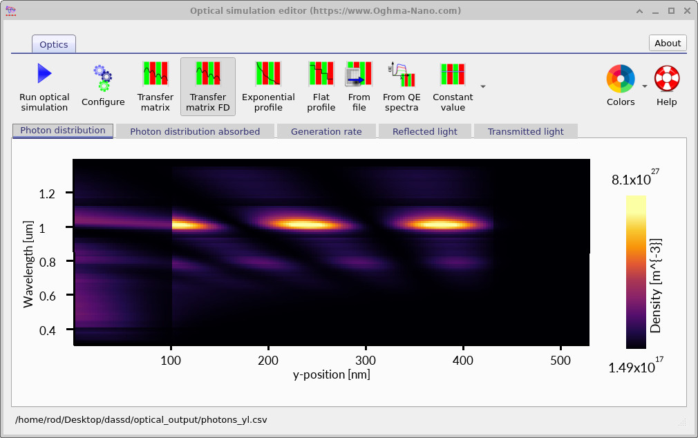
The plot in ?? is a wavelength–depth map. The horizontal axis is depth into the device (labelled y-position), and the vertical axis is wavelength. Bright colours near the illuminated surface indicate a high photon population; the fading with depth indicates absorption within the stack.
For a-Si:H, absorption in the visible is strong, so a large fraction of useful photons are absorbed within a relatively short distance from the front. The longer-wavelength limit is controlled by the a-Si:H effective bandgap: photons below the bandgap do not generate carriers efficiently, so the photon map will show a spectral boundary beyond which absorption and generation drop strongly. This is one reason thin-film a-Si:H devices typically trade absolute Jsc for higher bandgap and improved spectral selectivity compared with crystalline silicon.
The optical editor provides several tabs because “photon density” is not the same thing as “generation rate”. The Photon distribution view tells you where the optical field exists. The Photon distribution absorbed and Generation rate tabs are the ones that matter for the electrical model: the absorbed photon map is converted into a depth-dependent electron–hole pair generation rate, which is the source term injected into the drift–diffusion equations. For this a-Si:H cell, the resulting generation profile is strongly front-loaded and confined to the thin absorber, which is exactly the regime where recombination and transport near open circuit become decisive for Voc.
6. Running the simulation, JV curves, and extracting parameters
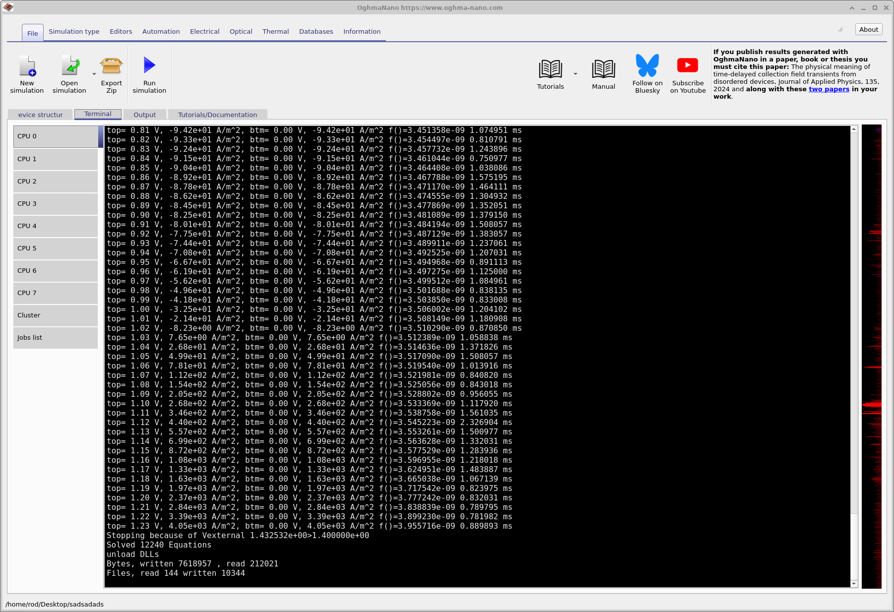
Once the device structure, electrical parameters, and optical generation are defined, the simulation can be run directly from the main window. Click the Run simulation button in the toolbar to start the solver. During execution, solver progress and convergence information are written to the terminal window (see ??).
For each bias point, the applied voltage at the top contact is listed first, followed by the resulting current density. Under illumination the current is initially negative (power generation). As the applied voltage is increased, the current magnitude decreases until it crosses zero at the open-circuit voltage. Beyond this point the current becomes positive, corresponding to forward-biased diode operation. The terminal output also reports the solver residual and convergence time for each bias step. Small residuals indicate that the coupled drift–diffusion and Poisson equations are being solved accurately.
jv.csv and siminfo.dat.
jv.csv. The curve shows negative current at low voltage,
a zero-current crossing at Voc, and forward conduction at higher bias.
siminfo.dat, listing extracted device metrics
such as Voc, Jsc, fill factor, and efficiency.
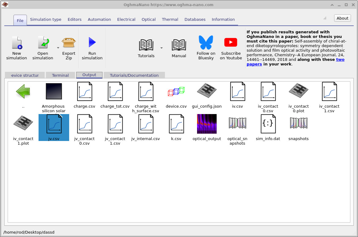
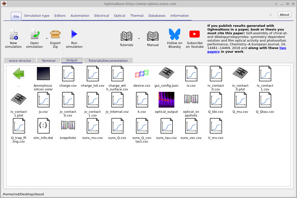
To inspect the electrical characteristics, open the Output tab and double-click
jv.csv. This displays the current density–voltage (JV) curve
(see ??).
The JV curve is the primary diagnostic of device behaviour: it should pass through the short-circuit current
at zero bias and cross zero current at the open-circuit voltage.
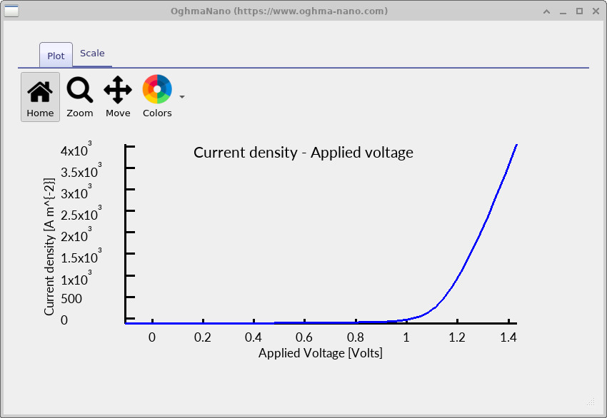
Double-clicking siminfo.dat opens the simulation information window
(see ??),
which reports extracted performance metrics, including fill factor, power conversion efficiency,
maximum power point, Voc, and Jsc.
Additional diagnostic quantities, such as free carrier densities at open circuit, are also useful for interpreting
defect-limited behaviour in a-Si:H.
A practical rule is to always inspect the JV curve before interpreting the numerical metrics.
If the JV curve does not pass cleanly through short circuit and open circuit, or if the current has an
unexpected sign or shape, the derived quantities in siminfo.dat will also be unreliable.
Visual inspection of the JV curve is the fastest way to diagnose configuration or modelling issues.
7. Suns–Voc analysis: recombination-limited voltage in a-Si:H
A Suns–Voc measurement probes how the open-circuit voltage evolves as a function of illumination intensity under strictly zero-current conditions. Because the terminal current is constrained to vanish, Suns–Voc isolates recombination physics from transport and contact resistance effects. The resulting curve is therefore one of the most direct diagnostics of voltage loss mechanisms in a solar cell.
In OghmaNano, Suns–Voc is implemented as a dedicated simulation mode. Instead of sweeping the applied voltage, the solver sweeps the illumination intensity and, at each intensity, adjusts the terminal voltage until the net current is zero. This directly computes the open-circuit operating point at each illumination level.
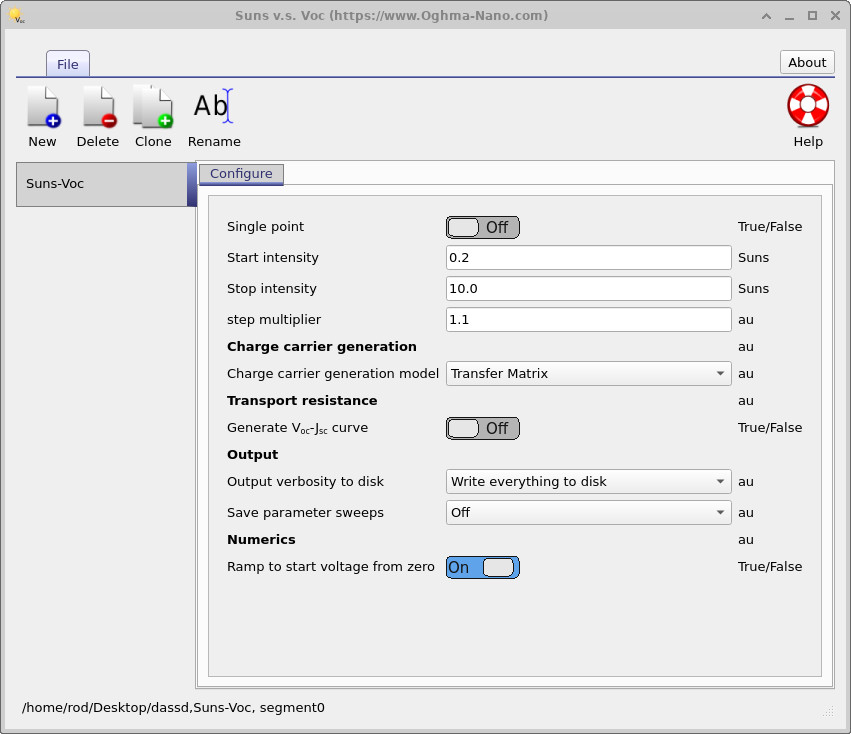
To enable Suns–Voc, open the Simulation type ribbon in the main window
(see ??)
and select Suns–Voc. Then click Run simulation.
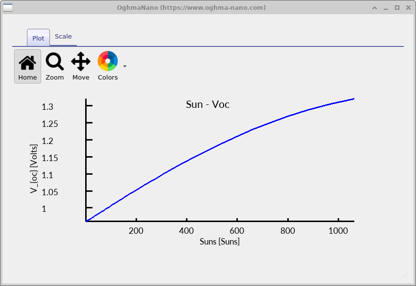
The solver automatically writes the results to disk; the file
suns_voc.csv contains Voc as a function of illumination intensity.
suns_voc.csv, charge_suns.csv, and tau_suns.csv files.
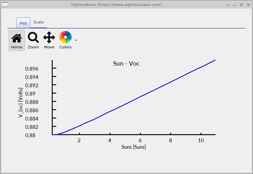
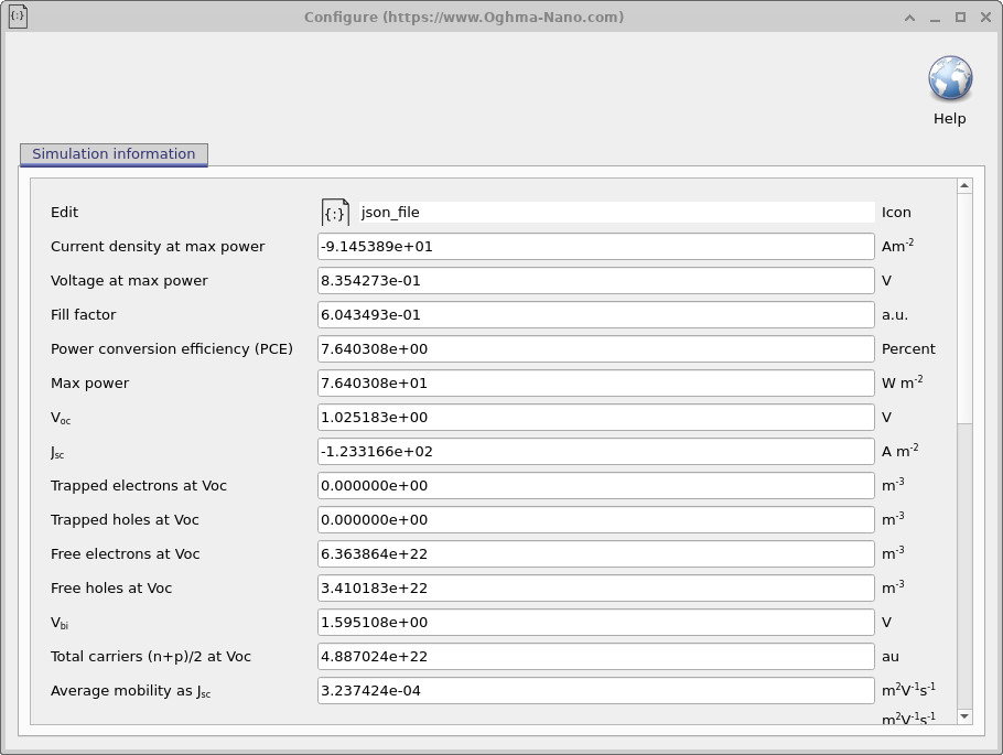
At low illumination, the increase in Voc is governed by the build-up of excess carrier density in the intrinsic absorber. In the non-degenerate limit, the quasi-Fermi level splitting is \[ qV_{\mathrm{oc}} = E_{Fn} - E_{Fp} = kT \ln\!\left(\frac{np}{n_i^2}\right), \] so Voc increases only logarithmically with carrier density.
In amorphous silicon, this low-intensity regime is often modified by defect occupation effects. At very low generation rates, a substantial fraction of photogenerated carriers are captured by deep and tail states before contributing to free-carrier populations. This can produce a weak or slightly flattened initial response in the Suns–Voc curve, as observed in ??. This behaviour is a physical consequence of trap filling rather than a numerical artefact.
To explore the high-injection regime, extend the illumination range. Open the Suns–Voc editor from the Editors ribbon and increase the stop intensity to 1000 suns. Rerun the simulation.
Opening suns_voc.csv after rerunning the simulation reveals the full
illumination range behaviour (see ??).
At high illumination, Voc continues to increase but with a steadily
decreasing slope, eventually approaching saturation.
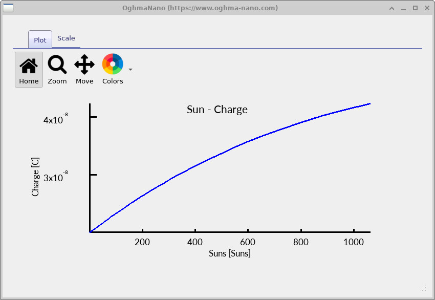
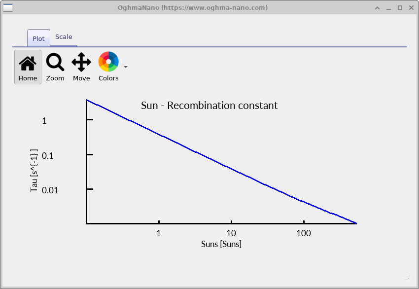
The origin of voltage saturation becomes clear when the Suns–Voc curve is viewed together with the stored charge and effective lifetime. As illumination increases, the total excess carrier density rises (see ??), but the effective recombination time simultaneously decreases (see ??).
In a-Si:H, recombination is dominated by defect-mediated SRH-type processes. As carrier density increases, trap-assisted recombination accelerates and the effective lifetime \[ \tau_{\mathrm{eff}} = \frac{\Delta n}{R} \] falls. Beyond this point, additional photogeneration primarily increases recombination rather than increasing the quasi-Fermi level separation.
This balance between generation and recombination imposes an intrinsic upper limit on Voc. The maximum voltage remains below the effective a-Si:H bandgap because recombination prevents the electron and hole quasi-Fermi levels from simultaneously approaching their respective band edges. The difference Eg/q − Voc therefore represents the fundamental recombination-induced voltage loss in this device.