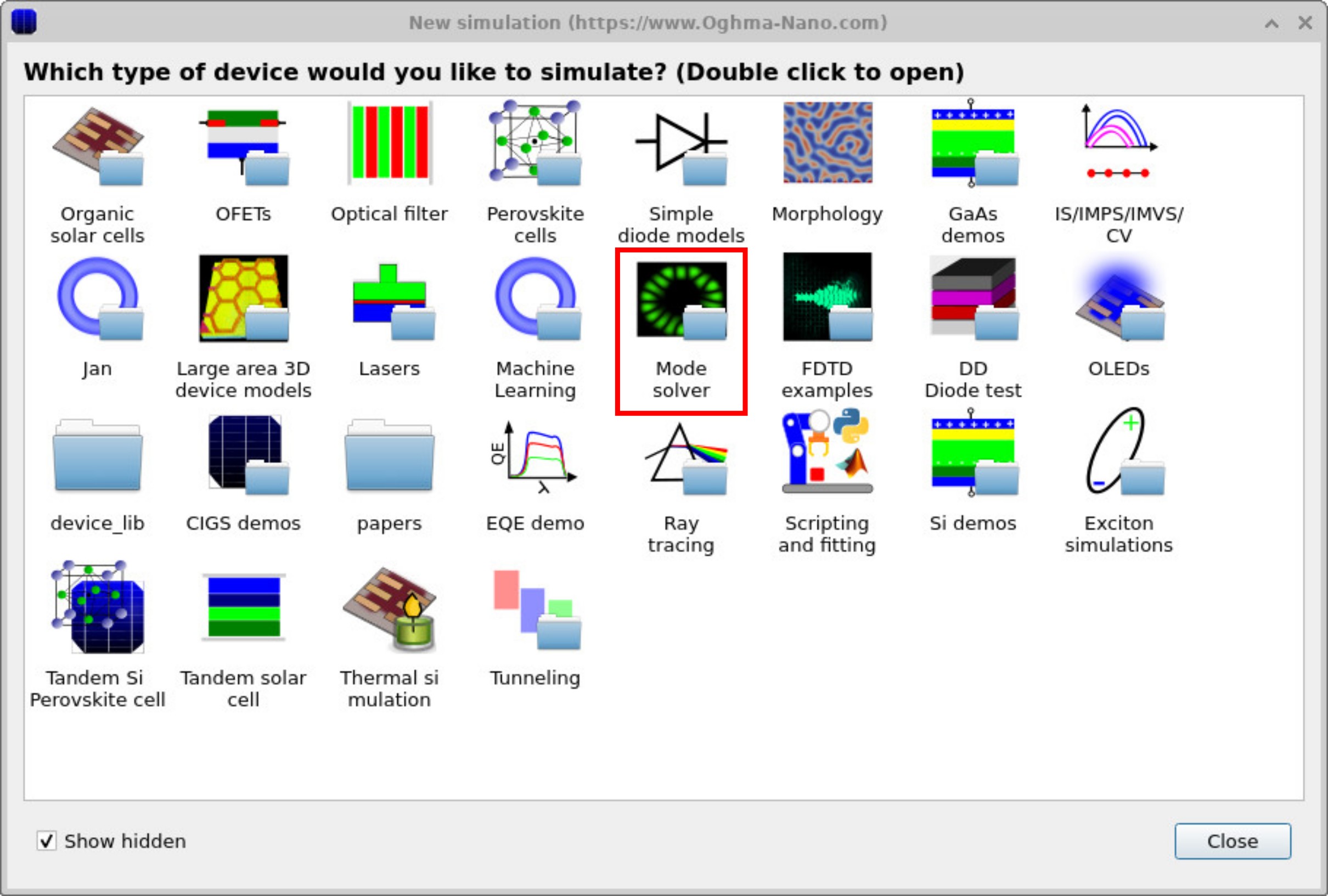
1D slab waveguide mode solver (TE/TM)
In this quick start we use OghmaNano’s mode solver to investigate the modal profiles of light in 1D slab waveguides, 2D slab waveguides, and 2D fiber-optic–type structures. We will examine both transverse electric (TE) and transverse magnetic (TM) modes supported by these structures. The solver finds guided modes by solving the eigenvalue problem below.
TE and TM mode equations
When a structure is about the same size as the wavelength of light, the light cannot spread freely but instead forms patterns called modes. These modes are trapped inside the structure by the difference in refractive index between layers and each mode has its own field pattern. The behaviour of light is given by these equations:
- TE modes: \[ \nabla_{\perp}^{2} E \;+\; \big(k_0^{2} n^{2} - \beta^{2}\big)\,E \;=\; 0 \]
- TM modes: \[ \nabla_{\perp}\!\cdot\!\!\left(\frac{1}{n^{2}}\,\nabla_{\perp} H\right) \;+\; \left(k_0^{2} - \frac{\beta^{2}}{n^{2}}\right)\,H \;=\; 0 \]
Where \( \nabla_{\perp} \) acts in the plane transverse to propagation (e.g., \(x\)–\(y\)), \(E\) and \(H\) are the out-of-plane field components for TE and TM formulations, \( n(x,y) \) is the (possibly wavelength-dependent) refractive index, \( k_0 \) is the free-space wavenumber, and \( \beta \) is the modal propagation constant that the solver determines along with the transverse field profiles.
Creating the waveguide simulation
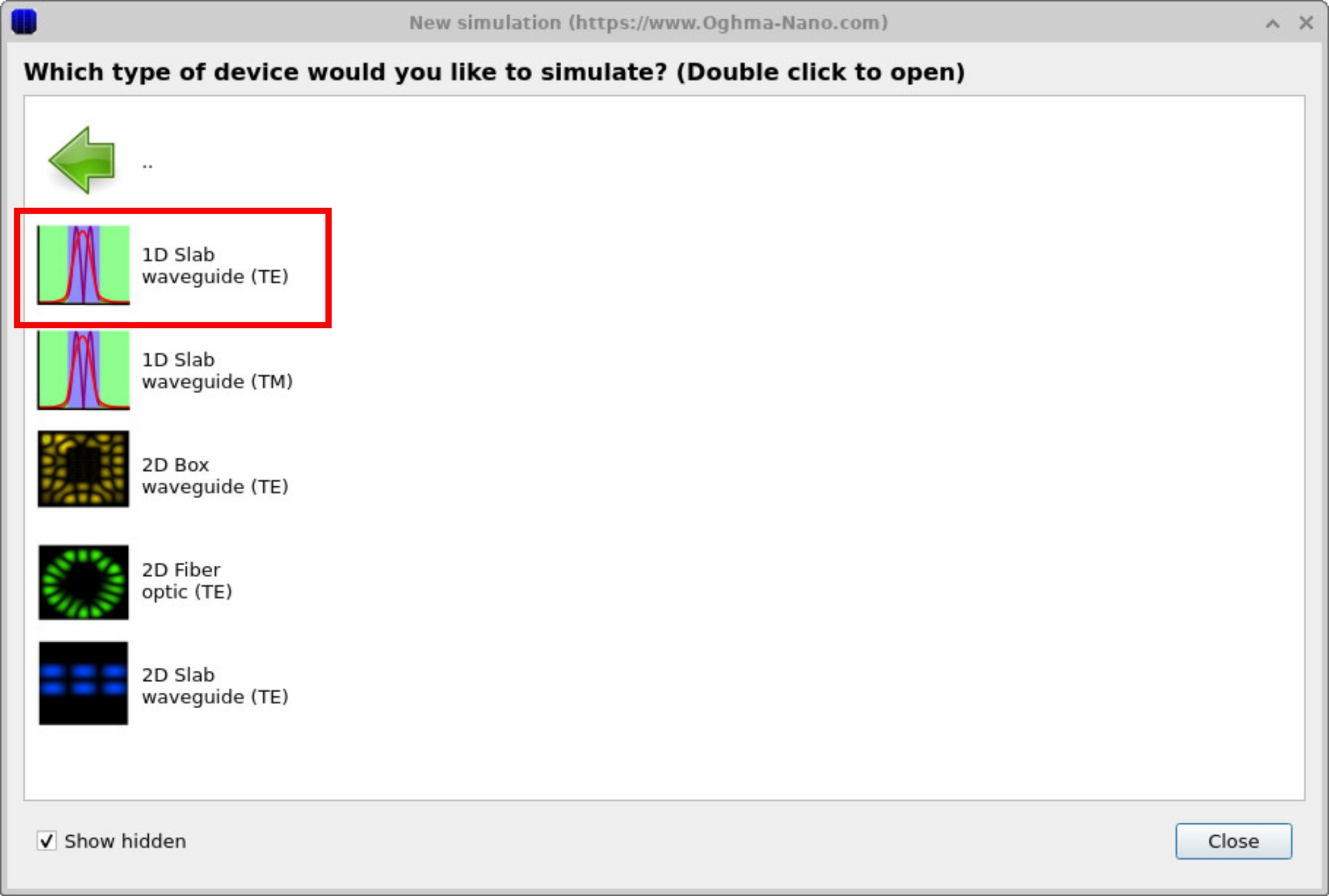
To start your first mode solver calculation, open the New simulations window from the File ribbon in the main window. Double-click on Mode Solver, and then double-click on 1D Slab Waveguide (TE), or transverse electric. Finally, save the new simulation to a folder on your disk.
1. Getting started: 1D slab (TE)
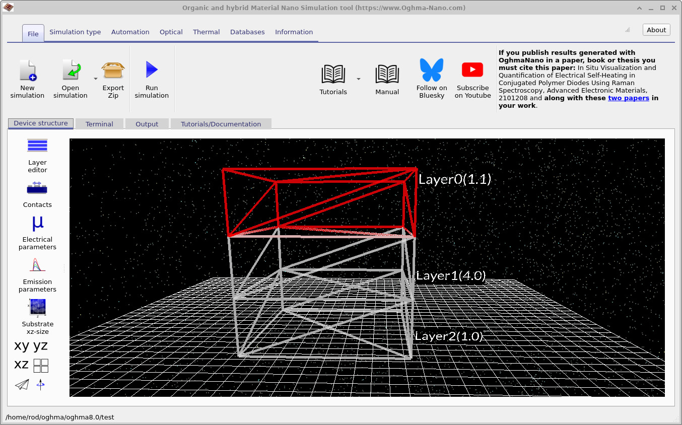
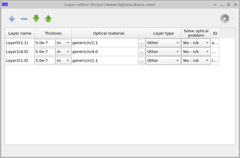
Once you have saved the simulation, the window in Figure 3 will appear. This shows a layer structure in the Epitaxy editor. The example consists of three layers: Layer 0, Layer 1, and Layer 2. The refractive index in Layer 1 is higher than in Layer 0 and Layer 2, forming a typical slab waveguide structure. Clicking the Play button starts the mode solver. The solver searches for modes supported within the structure. Because the solutions to the equations only exist at certain discrete wavelengths, not every wavelength will be supported. The Play button tells the solver to look for these supported modes.
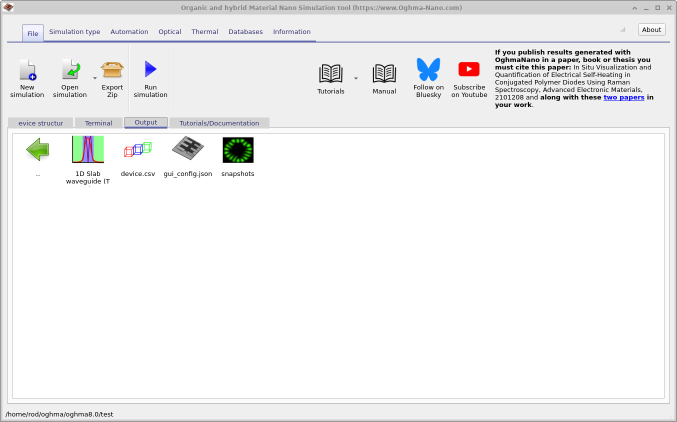
The time taken depends on the wavelength range you choose and the complexity of your structure, so the search can take a little while. Once the search is complete, an outputs directory is created containing a snapshots folder (see Figure 4). By double-clicking on this folder, you can view the modes that the solver has found.
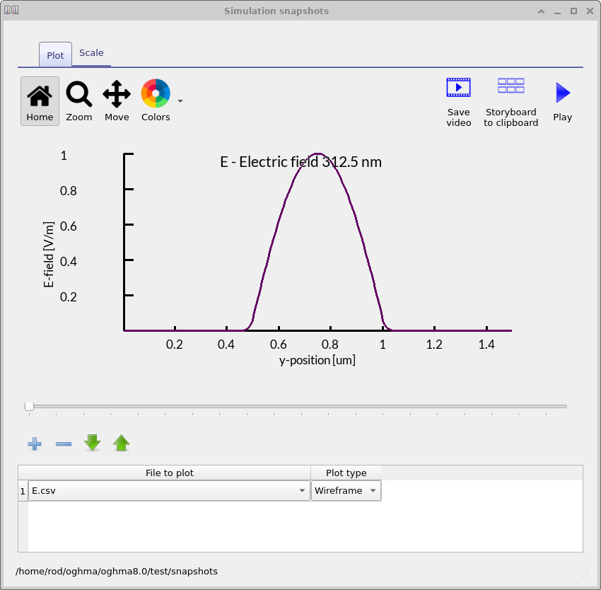
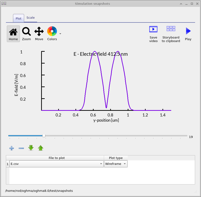
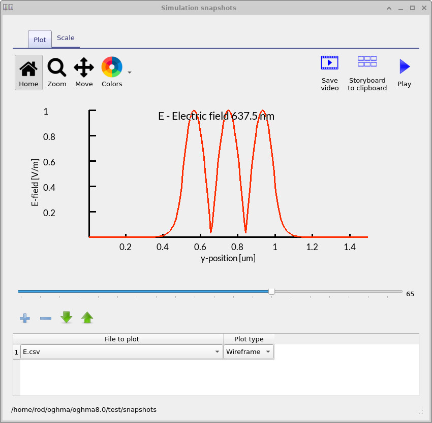
In Figures 5, 6, and 7 you can see three modes that the solver has found.
To view these results, open the snapshots folder, then click the plus button
and add E.csv to the list of fields to display.
Using the sliders, you can move through the different modes that were calculated.
The solver will show you which modes exist in the structure and what their field profiles look like.
Here, we show the first three harmonic modes that were found in the slab waveguide structure. These modes illustrate how light can be confined and guided in the device, depending on wavelength and geometry.
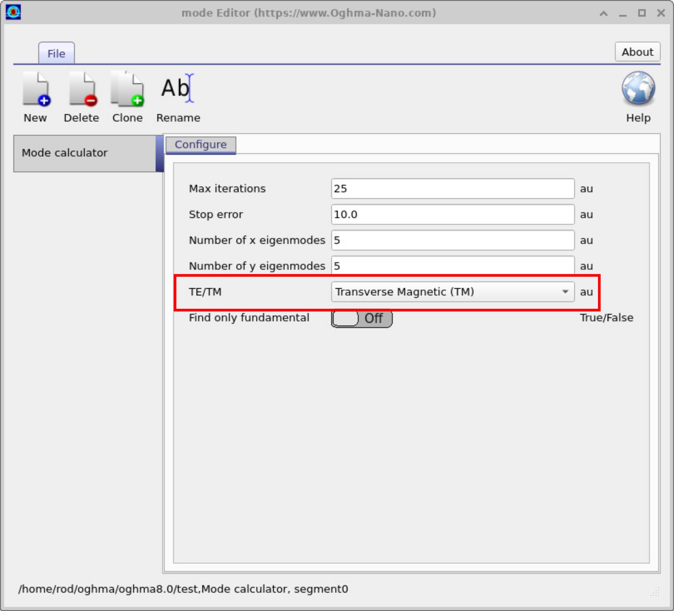
2. Switching to TM
In Optical → Mode calculator, change polarization to Transverse magnetic (TM), re-run, and reopen Snapshots. Due to boundary conditions at dielectric interfaces, TM modes show a characteristic field discontinuity at material boundaries (from continuity of D⊥ rather than E⊥). You should see slightly sharper jumps at core/cladding interfaces compared to TE.
6. Next steps
- Vary core thickness and index contrast to see cut-off behavior of higher-order modes.
- Increase wavelength sampling for smoother dispersion plots.
- Switch to TM in 2D and compare confinement vs. TE.
- Try the “more complex 2D waveguides” templates (rib/strip) for realistic photonics layouts.
👉 Next step: Continue to Part B to set up and solve 2D slab waveguides, including mesh definition, wavelength sampling, and eigenmode searches.