FDTD tutorial: Double slit (continuous sine wave)
1. Introduction
The double-slit experiment is the classic demonstration that light behaves as a wave. A coherent source illuminates two narrow apertures, and the transmitted fields spread into the region beyond the slits. Because both apertures emit coherent wavefronts, they interfere: regions where the phase aligns form intensity maxima, while regions with opposite phase form minima. The result is a characteristic fan-shaped diffraction pattern modulated by interference fringes.
You will run the built-in Double slit example, confirm that an OpenCL device is detected (so the simulation can run on a GPU when available), and then inspect the power-density snapshots to see the wavefronts diffract through the two openings and form the expected interference pattern in the free-space region.
2. Making a new simulation
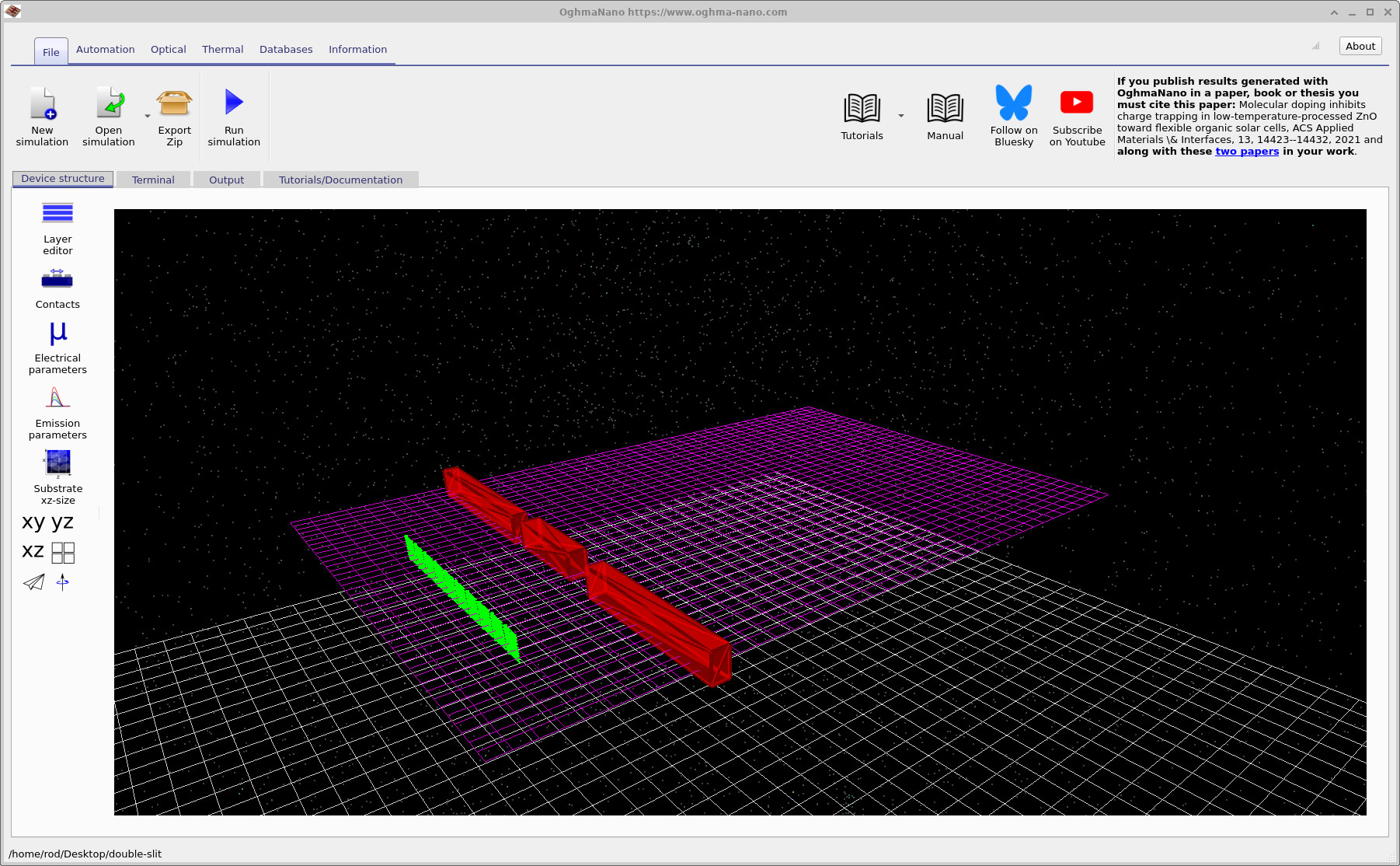
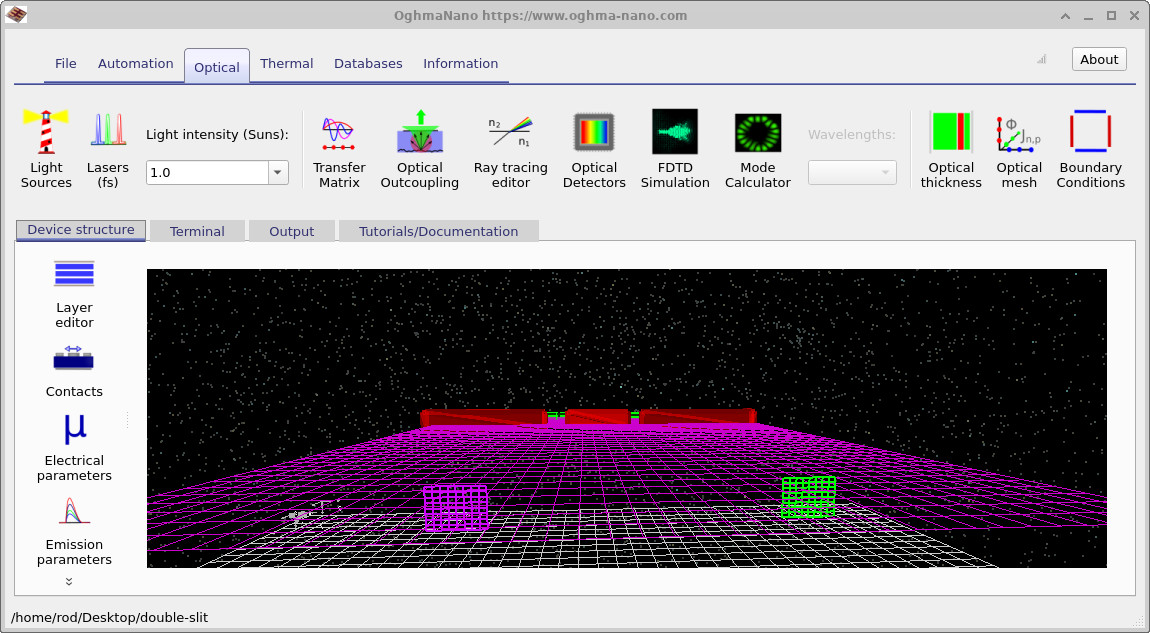
Start from the main OghmaNano window and click New simulation. In the New simulation browser, double-click FDTD examples, and then double-click Double slit (??, ??). This will open the main simulation window shown in ??.


3. Orienting yourself in the main window
After loading the example, the geometry is shown in the Device structure tab (??). The Terminal tab displays solver output during execution, including grid spacing, timestep, and which OpenCL device has been selected. The Output tab lists the files produced by the simulation, including the snapshots directory that contains time-dependent power-density data.

4. Running the simulation
Start the calculation by clicking Run simulation (▶) or pressing F9. The solver output appears in the Terminal tab (??). In this example you can see a green status line indicating that OghmaNano is searching for OpenCL devices, and that an OpenCL device has been found and selected.
This is important for performance. If an OpenCL-capable GPU is available (integrated or discrete), OghmaNano can run the FDTD update steps on the GPU rather than the CPU, which is typically significantly faster for these grid-based calculations. Most modern computers provide at least one OpenCL device, so in many cases you will see a device selected automatically. If no compatible device is found, the simulation still runs on the CPU; it will simply take longer.
5. Inspecting outputs
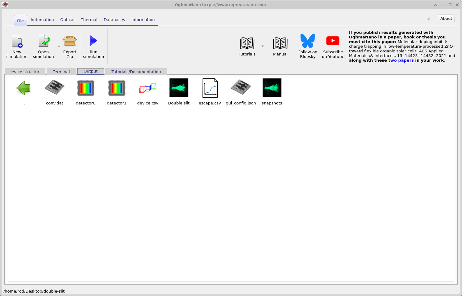
When the run completes, open the Output tab to view the files generated by the simulation. The output listing is shown in
??.
From here you can open the snapshots/ folder, which contains the time-dependent field-derived quantities
saved during the run.

snapshots/ to view time-domain power-density snapshots.
6. Viewing power density snapshots
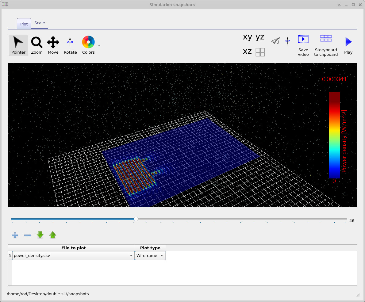
Double-click the snapshots/ directory in the Output tab to open the snapshot viewer. Then select
power_density.csv as the file to plot. The slider at the bottom of the viewer steps through time, letting you
watch how the electromagnetic energy density evolves as the simulation progresses.
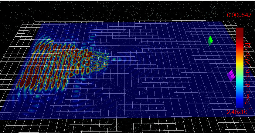
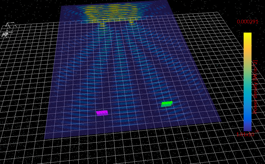
The sequence shown in ??– ?? illustrates the expected physics. The continuous sine wave launches into the structure, reaches the two apertures, and then diffracts into the region beyond the slits. Because there are two coherent emitters, the spreading wavefronts overlap and interfere, producing a fan-shaped diffraction region with alternating bands corresponding to constructive and destructive interference.
The snapshot viewer colour scheme can be changed by clicking Colors. This does not change the simulation result; it only changes how the same data is mapped to the displayed palette. For publications or teaching, it can be useful to switch palettes so the interference fringes are easier to see against the background.


7. Interpreting what you see
The key feature of the double-slit result is the combination of two effects. First, each aperture produces diffraction, so even a single slit would broaden the transmitted field into a spreading distribution. Second, because there are two apertures fed by the same coherent source, the transmitted fields remain phase-related, so their superposition produces interference fringes. In the snapshots this appears as a structured pattern in the region beyond the slits, where bands of high power density are separated by lower-power regions.
In a continuous sine-wave (CW) run, there is typically an initial transient as the domain fills with the injected field, followed by a regime where the field oscillates sinusoidally and the power-density pattern appears stable in time when viewed at the snapshot cadence. If you see strong spurious reflections, unexpected bright bands near boundaries, or an unstable growing field, the usual suspects are boundary conditions, insufficient absorbing layer thickness, or a timestep that is too aggressive for the chosen grid resolution.
8. Quick checks and common failure modes
- Unexpected reflections: verify that absorbing boundaries (CPML) are enabled and sufficiently thick, and that sources are not too close to the boundary.
- Pattern looks “blocky” or distorted: increase spatial resolution near the slits, because sharp features are most sensitive to grid dispersion.
- Slow execution: check the Terminal output for OpenCL device selection; if the run is on CPU, it will be slower.
- No clear interference fan: ensure the excitation is coherent and that you are plotting
power_density.csvfromsnapshots/rather than an unrelated output.
9. Enabling optical detectors
The double-slit example can optionally record the optical power incident on user-defined detector regions. These detectors act like small monitoring windows placed in the simulation domain: during the run, OghmaNano integrates the power crossing each detector area and saves a time trace to the output directory.
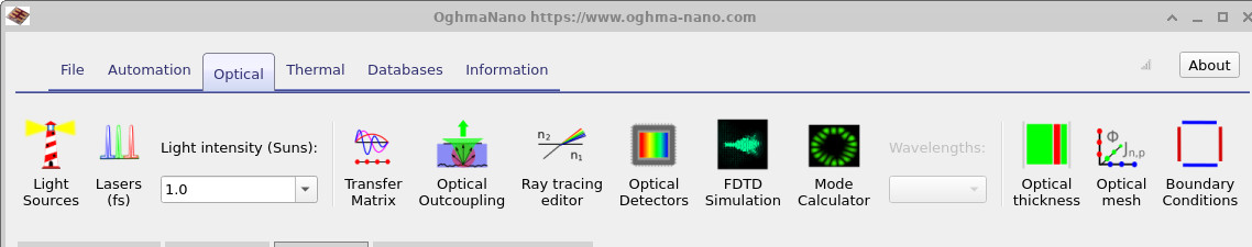
To enable detectors, navigate to the Optical ribbon and locate the Optical Detectors button, which is shown with a CCD-style camera icon (??).
Clicking Optical Detectors opens the detector editor. In this example there are two detectors (named one and two) and both are initially disabled. When a detector is disabled, the toolbar shows a red Disabled state. Click the disabled button to enable it; the indicator turns green to show the detector is active (??, ??). Repeat this for the second detector so both are enabled.
In the detector editor you can also see the detector’s position (x, y, z) and its size in micrometres. For this tutorial you do not need to change any of these values; the example is preconfigured to demonstrate an important physical point: one detector sits in a region of high diffracted intensity, while the other sits in a region where the diffracted field is comparatively weak.


10. Rerun and view detector outputs
After enabling the detectors, rerun the simulation (▶ or F9). When the run completes, open the Output tab.
You should now see two additional output entries corresponding to the detector results (for example detector0 and
detector1), as shown in
??.
Double-click each detector entry to open its power-versus-time plot
(??,
??).


The difference between the two traces is easiest to understand by comparing their vertical scales. One detector records power at the level of only a few microwatts (or less), while the other records a substantially larger signal once the diffracted field reaches it. The delayed onset in both traces is expected: the simulation begins at t=0 with the source turning on, and the detectors cannot respond until the electromagnetic wave has propagated from the source, through the slits, and across the free-space region to their locations.
11. Physical interpretation: detectors and diffraction lobes
The purpose of placing two detectors is to connect the time-domain data to the spatial diffraction pattern. In a double-slit system, the far-field structure is not uniform: there are directions in which the two slit contributions add constructively (high intensity), and directions in which they add destructively (low intensity). In other words, the diffracted field forms lobes and troughs, and the measured detector power depends strongly on whether the detector sits in a bright region or in a null.
This is visible directly in the snapshot view with detectors present (??). One detector lies in the path of a strong diffracted lobe and therefore accumulates significant optical power. The other detector lies in a region where the interference is predominantly destructive (a trough of the pattern), so comparatively little power crosses its monitor area. This is why the two output traces differ by orders of magnitude even though the detectors are otherwise identical objects.
Conceptually, this is the same physics used in optical metrology and imaging: a detector does not measure an abstract “total power” of the simulation, it measures whatever portion of the field crosses its finite area in its specific location. Moving the detector by only a small distance can shift it from a bright fringe into a neighbouring dark fringe, which can change the measured power dramatically. In practical systems, this sensitivity is exactly why diffraction and interference patterns are useful: they encode geometric information (slit spacing, aperture size, wavelength) into measurable intensity distributions.
12. Adjusting the slit
One advantage of a numerical FDTD experiment is that the geometry can be modified interactively and the resulting optical behaviour can be explored immediately. In this section we modify the position of the central blocking element that forms the double-slit aperture and observe how this changes the diffraction pattern and the power detected by the two optical detectors.
Using the mouse in the 3D device window, select the centre block that forms the double slit and drag it toward the left-hand side of the structure as shown in ??. Normally objects cannot pass through each other while being dragged, but if the block collides with another object you can hold down the Shift key while dragging. This allows the block to pass through other geometry so it can be repositioned easily.
After moving the block, rerun the simulation (▶ or F9). The resulting optical field distribution is shown in ??.


In this configuration the optical beam no longer splits into two comparable diffracting sources. Instead, the light passes predominantly through a single opening and propagates forward in a more collimated manner. Some diffraction still occurs, because any finite aperture produces spreading according to wave optics, but the interference pattern that was previously produced by two coherent slits is now much weaker. As a consequence, the detectors receive very little optical power compared with the original geometry.
13. Moving the block toward the source
Next we modify the geometry in a different way. Using the mouse again, drag the centre block backward toward the optical source as shown in ??. As before, you can hold the Shift key while dragging to allow the block to pass through other objects if necessary.
Once the block has been repositioned, rerun the simulation. The resulting field distribution is shown in ??.


Moving the blocking element closer to the source alters the effective aperture geometry and therefore changes the spatial distribution of the transmitted optical field. Because diffraction depends sensitively on the shape and position of the aperture relative to the incoming wavefront, even relatively small geometric changes can significantly modify the resulting interference structure. In this case the diffracted beams emerge at different angles and the interference pattern changes accordingly.
This demonstrates a key feature of wave optics simulations: diffraction patterns are determined entirely by geometry and wavelength. By modifying the physical layout of the structure, you can explore how aperture shape, slit separation, and obstacle placement affect the resulting optical field distribution and the power measured by detectors placed within the simulation domain.
14. Adding a lens using the mesh editor
In the previous sections we explored how changing the aperture geometry changes the diffraction pattern. In this final section we go one step further and demonstrate how to transform a simple object into a more complex mesh using the Mesh editor. This is a powerful workflow in OghmaNano: you can start with simple primitives to build intuition, then progressively introduce more realistic optical components such as lenses, curved surfaces, and imported CAD meshes.
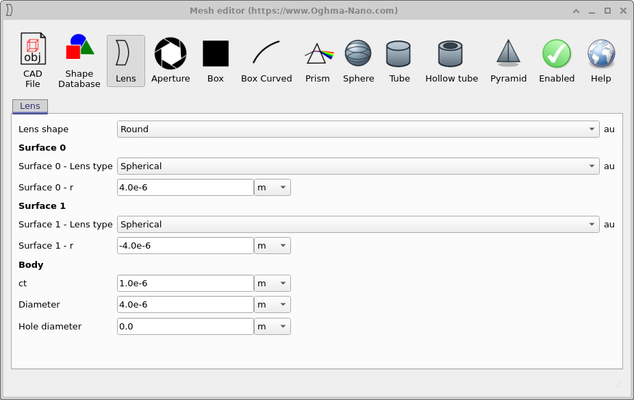
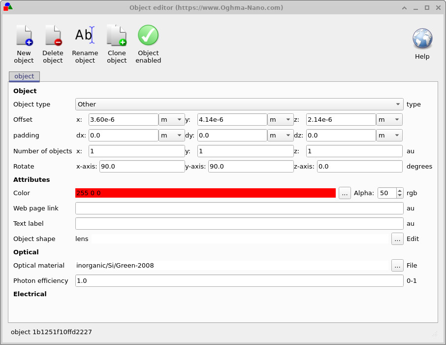
First, reorient the device view so it matches ??. Then right-click on the centre block of the double-slit structure and open the Mesh editor. This opens the editor shown in ??. In the mesh editor, click the Lens button and enter the parameters exactly as shown in ??.
With these values you can generate a lens-shaped object. If you leave the lens in its default orientation it will appear as a “flat” lens in the device view, as shown in ??. For this tutorial we do not want the lens lying flat in the simulation plane, because the optical field will not interact with it in a meaningful way. The lens needs to be rotated so it stands upright and intercepts the propagating wavefront.


15. Rotating the lens and setting an optical material
To rotate the new lens object, right-click on the lens and open the Object editor. This opens the editor shown in ??. Set the rotation angles to 90, 90, and 0 (x, y, z) exactly as shown. This rotates the lens so it stands upright in the propagation path and can interact strongly with the incoming field.
While you are in the object editor, make the lens optically transparent by selecting the optical material shown in the figure: inorganic/Si/Green-2008. This is a convenient wideband refractive-index profile for silicon, suitable for demonstrating refraction and focusing behaviour. With this material assigned, the lens becomes a true refractive object rather than simply a geometric blocker.
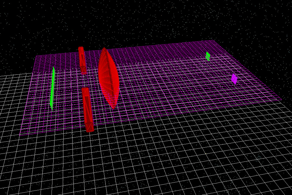
After setting the rotation and material, the geometry should look like ??, where the lens stands vertically in the simulation region.
16. Running the FDTD simulation with the lens
Rerun the simulation with the lens present. A representative power-density snapshot is shown in ??. You can clearly see the incoming wavefront interacting with the curved refractive surface: part of the field is transmitted through the lens and refracted, and part is reflected back toward the source.
The transmitted field forms a region of much denser wavefront structure in and around the lens, and the outgoing field shows evidence of focusing: the transmitted energy is concentrated toward a smaller region rather than continuing to spread freely as in the bare-aperture case. At the same time, the reflection from the lens sends a significant fraction of the optical power back toward the aperture region, which reduces the amount of power reaching the detectors placed downstream. This is exactly what you would expect physically: a refractive element introduces impedance mismatch at its interfaces, and unless the lens is anti-reflection coated or index-matched, Fresnel reflection can be substantial.
This example illustrates why “mesh transformation” tools matter in practical simulations. Even simple systems quickly become dominated by curved surfaces and engineered optical components. Being able to turn a basic block into a lens (or any other mesh object) lets you build optics directly inside the same workflow used for FDTD. The same approach can be used to create and study microlenses, concentrators, diffractive optical elements, wavefront-shaping structures, or imported CAD geometries for realistic devices.